-
 A KAIST Research Team Develops a Novel “Bone Bandage” Material for Cracked Bones
Bone regeneration is a complex process, and existing methods to aid regeneration including transplants and growth factor transmissions face limitations such as the high cost. But recently, a piezoelectric material that can promote the growth of bone tissue has been developed.
A KAIST research team led by Professor Seungbum Hong from the Department of Materials Science and Engineering (DMSE) announced on January 25 the development of a biomimetic scaffold that generates electrical signals upon the application of pressure by utilizing the unique osteogenic ability of hydroxyapatite (HAp). This research was conducted in collaboration with a team led by Professor Jangho Kim from the Department of Convergence Biosystems Engineering at Chonnam National University.
HAp is a basic calcium phosphate material found in bones and teeth. This biocompatible mineral substance is also known to prevent tooth decay and is often used in toothpaste.
Previous studies on piezoelectric scaffolds confirmed the effects of piezoelectricity on promoting bone regeneration and improving bone fusion in various polymer-based materials, but were limited in simulating the complex cellular environment required for optimal bone tissue regeneration. However, this research suggests a new method for utilizing the unique osteogenic abilities of HAp to develop a material that mimics the environment for bone tissue in a living body.
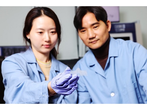
< Figure 1. Design and characterization of piezoelectrically and topographically originated biomimetic scaffolds. (a) Schematic representation of the enhanced bone regeneration mechanism through electrical and topographical cues provided by HAp-incorporated P(VDF-TrFE) scaffolds. (b) Schematic diagram of the fabrication process. >
The research team developed a manufacturing process that fuses HAp with a polymer film. The flexible and free-standing scaffold developed through this process demonstrated its remarkable potential for promoting bone regeneration through in-vitro and in-vivo experiments in rats.
The team also identified the principles of bone regeneration that their scaffold is based on. Using atomic force microscopy (AFM), they analysed the electrical properties of the scaffold and evaluated the detailed surface properties related to cell shape and cell skeletal protein formation. They also investigated the effects of piezoelectricity and surface properties on the expression of growth factors.
Professor Hong from KAIST’s DMSE said, “We have developed a HAp-based piezoelectric composite material that can act like a ‘bone bandage’ through its ability to accelerate bone regeneration.” He added, “This research not only suggests a new direction for designing biomaterials, but is also significant in having explored the effects of piezoelectricity and surface properties on bone regeneration.”
This research, conducted by co-first authors Soyun Joo and Soyeon Kim from Professor Hong’s group, was published on ACS Applied Materials & Interfaces on January 4 under the title “Piezoelectrically and Topographically Engineered Scaffolds for Accelerating Bone Regeneration”. From Professor Kim’s group, Ph.D. candidate Yonghyun Gwon also participated as co-first author, and Professor Kim himself as a corresponding author.
< Figure 2. Analysis of piezoelectric and surface properties of the biomimetic scaffolds using atomic force microscopy. (a) PFM amplitude and phase images of box-poled composite scaffolds. The white bar represents 2 μm. (b) 3D representations of composite scaffolds paired with typical 2D line sections. (c) In vivo bone regeneration micro-CT analysis, (d) schematic representation of filler-derived electrical origins in bone regeneration. >
This research was supported by the KAIST Research and Development Team, the KUSTAR-KAIST Joint Research Center, the KAIST Global Singularity Project, and the government-funded Basic Research Project by the National Research Foundation of Korea.
2024.02.01 View 2649
A KAIST Research Team Develops a Novel “Bone Bandage” Material for Cracked Bones
Bone regeneration is a complex process, and existing methods to aid regeneration including transplants and growth factor transmissions face limitations such as the high cost. But recently, a piezoelectric material that can promote the growth of bone tissue has been developed.
A KAIST research team led by Professor Seungbum Hong from the Department of Materials Science and Engineering (DMSE) announced on January 25 the development of a biomimetic scaffold that generates electrical signals upon the application of pressure by utilizing the unique osteogenic ability of hydroxyapatite (HAp). This research was conducted in collaboration with a team led by Professor Jangho Kim from the Department of Convergence Biosystems Engineering at Chonnam National University.
HAp is a basic calcium phosphate material found in bones and teeth. This biocompatible mineral substance is also known to prevent tooth decay and is often used in toothpaste.
Previous studies on piezoelectric scaffolds confirmed the effects of piezoelectricity on promoting bone regeneration and improving bone fusion in various polymer-based materials, but were limited in simulating the complex cellular environment required for optimal bone tissue regeneration. However, this research suggests a new method for utilizing the unique osteogenic abilities of HAp to develop a material that mimics the environment for bone tissue in a living body.
< Figure 1. Design and characterization of piezoelectrically and topographically originated biomimetic scaffolds. (a) Schematic representation of the enhanced bone regeneration mechanism through electrical and topographical cues provided by HAp-incorporated P(VDF-TrFE) scaffolds. (b) Schematic diagram of the fabrication process. >
The research team developed a manufacturing process that fuses HAp with a polymer film. The flexible and free-standing scaffold developed through this process demonstrated its remarkable potential for promoting bone regeneration through in-vitro and in-vivo experiments in rats.
The team also identified the principles of bone regeneration that their scaffold is based on. Using atomic force microscopy (AFM), they analysed the electrical properties of the scaffold and evaluated the detailed surface properties related to cell shape and cell skeletal protein formation. They also investigated the effects of piezoelectricity and surface properties on the expression of growth factors.
Professor Hong from KAIST’s DMSE said, “We have developed a HAp-based piezoelectric composite material that can act like a ‘bone bandage’ through its ability to accelerate bone regeneration.” He added, “This research not only suggests a new direction for designing biomaterials, but is also significant in having explored the effects of piezoelectricity and surface properties on bone regeneration.”
This research, conducted by co-first authors Soyun Joo and Soyeon Kim from Professor Hong’s group, was published on ACS Applied Materials & Interfaces on January 4 under the title “Piezoelectrically and Topographically Engineered Scaffolds for Accelerating Bone Regeneration”. From Professor Kim’s group, Ph.D. candidate Yonghyun Gwon also participated as co-first author, and Professor Kim himself as a corresponding author.
< Figure 2. Analysis of piezoelectric and surface properties of the biomimetic scaffolds using atomic force microscopy. (a) PFM amplitude and phase images of box-poled composite scaffolds. The white bar represents 2 μm. (b) 3D representations of composite scaffolds paired with typical 2D line sections. (c) In vivo bone regeneration micro-CT analysis, (d) schematic representation of filler-derived electrical origins in bone regeneration. >
This research was supported by the KAIST Research and Development Team, the KUSTAR-KAIST Joint Research Center, the KAIST Global Singularity Project, and the government-funded Basic Research Project by the National Research Foundation of Korea.
2024.02.01 View 2649 -
 KAIST Research Team Develops Sweat-Resistant Wearable Robot Sensor
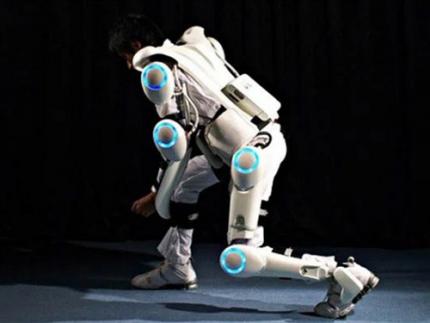
New electromyography (EMG) sensor technology that allows the long-term stable control of wearable robots and is not affected by the wearer’s sweat and dead skin has gained attention recently. Wearable robots are devices used across a variety of rehabilitation treatments for the elderly and patients recovering from stroke or trauma.
A joint research team led by Professor Jae-Woong Jung from the KAIST School of Electrical Engineering (EE) and Professor Jung Kim from the KAIST Department of Mechanical Engineering (ME) announced on January 23rd that they have successfully developed a stretchable and adhesive microneedle sensor that can electrically sense physiological signals at a high level without being affected by the state of the user’s skin.
For wearable robots to recognize the intentions behind human movement for their use in rehabilitation treatment, they require a wearable electrophysiological sensor that gives precise EMG measurements. However, existing sensors often show deteriorating signal quality over time and are greatly affected by the user’s skin conditions. Furthermore, the sensor’s higher mechanical hardness causes noise since the contact surface is unable to keep up with the deformation of the skin. These shortcomings limit the reliable, long-term control of wearable robots.
< Figure 1. Design and working concept of the Stretchable microNeedle Adhesive Patch (SNAP). (A) Schematic illustration showing the overall system configuration and application of SNAP. (B) Exploded view schematic diagram of a SNAP, consisting of stretchable serpentine interconnects, Au-coated Si microneedle, and ECA made of Ag flakes–silicone composite. (C) Optical images showing high mechanical compliance of SNAP. >
However, the recently developed technology is expected to allow long-term and high-quality EMG measurements as it uses a stretchable and adhesive conducting substrate integrated with microneedle arrays that can easily penetrate the stratum corneum without causing discomfort. Through its excellent performance, the sensor is anticipated to be able to stably control wearable robots over a long period of time regardless of the wearer’s changing skin conditions and without the need for a preparation step that removes sweat and dead cells from the surface of their skin.
The research team created a stretchable and adhesive microneedle sensor by integrating microneedles into a soft silicon polymer substrate. The hard microneedles penetrate through the stratum corneum, which has high electrical resistance. As a result, the sensor can effectively lower contact resistance with the skin and obtain high-quality electrophysiological signals regardless of contamination. At the same time, the soft and adhesive conducting substrate can adapt to the skin’s surface that stretches with the wearer’s movement, providing a comfortable fit and minimizing noise caused by movement.
< Figure 2. Demonstration of the wireless Stretchable microNeedle Adhesive Patch (SNAP) system as an Human-machine interfaces (HMI) for closed-loop control of an exoskeleton robot. (A) Illustration depicting the system architecture and control strategy of an exoskeleton robot. (B) The hardware configuration of the pneumatic back support exoskeleton system. (C) Comparison of root mean square (RMS) of electromyography (EMG) with and without robotic assistance of pretreated skin and non-pretreated skin. >
To verify the usability of the new patch, the research team conducted a motion assistance experiment using a wearable robot. They attached the microneedle patch on a user’s leg, where it could sense the electrical signals generated by the muscle. The sensor then sent the detected intention to a wearable robot, allowing the robot to help the wearer lift a heavy object more easily.
Professor Jae-Woong Jung, who led the research, said, “The developed stretchable and adhesive microneedle sensor can stability detect EMG signals without being affected by the state of a user’s skin. Through this, we will be able to control wearable robots with higher precision and stability, which will help the rehabilitation of patients who use robots.”
The results of this research, written by co-first authors Heesoo Kim and Juhyun Lee, who are both Ph.D. candidates in the KAIST School of EE, were published in Science Advances on January 17th under the title “Skin-preparation-free, stretchable microneedle adhesive patches for reliable electrophysiological sensing and exoskeleton robot control”.
This research was supported by the Bio-signal Sensor Integrated Technology Development Project by the National Research Foundation of Korea, the Electronic Medicinal Technology Development Project, and the Step 4 BK21 Project.
2024.01.30 View 2474
KAIST Research Team Develops Sweat-Resistant Wearable Robot Sensor
New electromyography (EMG) sensor technology that allows the long-term stable control of wearable robots and is not affected by the wearer’s sweat and dead skin has gained attention recently. Wearable robots are devices used across a variety of rehabilitation treatments for the elderly and patients recovering from stroke or trauma.
A joint research team led by Professor Jae-Woong Jung from the KAIST School of Electrical Engineering (EE) and Professor Jung Kim from the KAIST Department of Mechanical Engineering (ME) announced on January 23rd that they have successfully developed a stretchable and adhesive microneedle sensor that can electrically sense physiological signals at a high level without being affected by the state of the user’s skin.
For wearable robots to recognize the intentions behind human movement for their use in rehabilitation treatment, they require a wearable electrophysiological sensor that gives precise EMG measurements. However, existing sensors often show deteriorating signal quality over time and are greatly affected by the user’s skin conditions. Furthermore, the sensor’s higher mechanical hardness causes noise since the contact surface is unable to keep up with the deformation of the skin. These shortcomings limit the reliable, long-term control of wearable robots.
< Figure 1. Design and working concept of the Stretchable microNeedle Adhesive Patch (SNAP). (A) Schematic illustration showing the overall system configuration and application of SNAP. (B) Exploded view schematic diagram of a SNAP, consisting of stretchable serpentine interconnects, Au-coated Si microneedle, and ECA made of Ag flakes–silicone composite. (C) Optical images showing high mechanical compliance of SNAP. >
However, the recently developed technology is expected to allow long-term and high-quality EMG measurements as it uses a stretchable and adhesive conducting substrate integrated with microneedle arrays that can easily penetrate the stratum corneum without causing discomfort. Through its excellent performance, the sensor is anticipated to be able to stably control wearable robots over a long period of time regardless of the wearer’s changing skin conditions and without the need for a preparation step that removes sweat and dead cells from the surface of their skin.
The research team created a stretchable and adhesive microneedle sensor by integrating microneedles into a soft silicon polymer substrate. The hard microneedles penetrate through the stratum corneum, which has high electrical resistance. As a result, the sensor can effectively lower contact resistance with the skin and obtain high-quality electrophysiological signals regardless of contamination. At the same time, the soft and adhesive conducting substrate can adapt to the skin’s surface that stretches with the wearer’s movement, providing a comfortable fit and minimizing noise caused by movement.
< Figure 2. Demonstration of the wireless Stretchable microNeedle Adhesive Patch (SNAP) system as an Human-machine interfaces (HMI) for closed-loop control of an exoskeleton robot. (A) Illustration depicting the system architecture and control strategy of an exoskeleton robot. (B) The hardware configuration of the pneumatic back support exoskeleton system. (C) Comparison of root mean square (RMS) of electromyography (EMG) with and without robotic assistance of pretreated skin and non-pretreated skin. >
To verify the usability of the new patch, the research team conducted a motion assistance experiment using a wearable robot. They attached the microneedle patch on a user’s leg, where it could sense the electrical signals generated by the muscle. The sensor then sent the detected intention to a wearable robot, allowing the robot to help the wearer lift a heavy object more easily.
Professor Jae-Woong Jung, who led the research, said, “The developed stretchable and adhesive microneedle sensor can stability detect EMG signals without being affected by the state of a user’s skin. Through this, we will be able to control wearable robots with higher precision and stability, which will help the rehabilitation of patients who use robots.”
The results of this research, written by co-first authors Heesoo Kim and Juhyun Lee, who are both Ph.D. candidates in the KAIST School of EE, were published in Science Advances on January 17th under the title “Skin-preparation-free, stretchable microneedle adhesive patches for reliable electrophysiological sensing and exoskeleton robot control”.
This research was supported by the Bio-signal Sensor Integrated Technology Development Project by the National Research Foundation of Korea, the Electronic Medicinal Technology Development Project, and the Step 4 BK21 Project.
2024.01.30 View 2474 -
 KAIST Professor Jiyun Lee becomes the first Korean to receive the Thurlow Award from the American Institute of Navigation
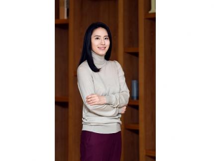
< Distinguished Professor Jiyun Lee from the KAIST Department of Aerospace Engineering >
KAIST (President Kwang-Hyung Lee) announced on January 27th that Distinguished Professor Jiyun Lee from the KAIST Department of Aerospace Engineering had won the Colonel Thomas L. Thurlow Award from the American Institute of Navigation (ION) for her achievements in the field of satellite navigation.
The American Institute of Navigation (ION) announced Distinguished Professor Lee as the winner of the Thurlow Award at its annual awards ceremony held in conjunction with its international conference in Long Beach, California on January 25th. This is the first time a person of Korean descent has received the award.
The Thurlow Award was established in 1945 to honor Colonel Thomas L. Thurlow, who made significant contributions to the development of navigation equipment and the training of navigators. This award aims to recognize an individual who has made an outstanding contribution to the development of navigation and it is awarded to one person each year. Past recipients include MIT professor Charles Stark Draper, who is well-known as the father of inertial navigation and who developed the guidance computer for the Apollo moon landing project.
Distinguished Professor Jiyun Lee was recognized for her significant contributions to technological advancements that ensure the safety of satellite-based navigation systems for aviation. In particular, she was recognized as a world authority in the field of navigation integrity architecture design, which is essential for ensuring the stability of intelligent transportation systems and autonomous unmanned systems. Distinguished Professor Lee made a groundbreaking contribution to help ensure the safety of satellite-based navigation systems from ionospheric disturbances, including those affected by sudden changes in external factors such as the solar and space environment.
She has achieved numerous scientific discoveries in the field of ionospheric research, while developing new ionospheric threat modeling methods, ionospheric anomaly monitoring and mitigation techniques, and integrity and availability assessment techniques for next-generation augmented navigation systems. She also contributed to the international standardization of technology through the International Civil Aviation Organization (ICAO).
Distinguished Professor Lee and her research group have pioneered innovative navigation technologies for the safe and autonomous operation of unmanned aerial vehicles (UAVs) and urban air mobility (UAM). She was the first to propose and develop a low-cost navigation satellite system (GNSS) augmented architecture for UAVs with a near-field network operation concept that ensures high integrity, and a networked ground station-based augmented navigation system for UAM. She also contributed to integrity design techniques, including failure monitoring and integrity risk assessment for multi-sensor integrated navigation systems.
< Professor Jiyoon Lee upon receiving the Thurlow Award >
Bradford Parkinson, professor emeritus at Stanford University and winner of the 1986 Thurlow Award, who is known as the father of GPS, congratulated Distinguished Professor Lee upon hearing that she was receiving the Thurlow Award and commented that her innovative research has addressed many important topics in the field of navigation and her solutions are highly innovative and highly regarded.
Distinguished Professor Lee said, “I am very honored and delighted to receive this award with its deep history and tradition in the field of navigation.” She added, “I will strive to help develop the future mobility industry by securing safe and sustainable navigation technology.”
2024.01.26 View 2026
KAIST Professor Jiyun Lee becomes the first Korean to receive the Thurlow Award from the American Institute of Navigation
< Distinguished Professor Jiyun Lee from the KAIST Department of Aerospace Engineering >
KAIST (President Kwang-Hyung Lee) announced on January 27th that Distinguished Professor Jiyun Lee from the KAIST Department of Aerospace Engineering had won the Colonel Thomas L. Thurlow Award from the American Institute of Navigation (ION) for her achievements in the field of satellite navigation.
The American Institute of Navigation (ION) announced Distinguished Professor Lee as the winner of the Thurlow Award at its annual awards ceremony held in conjunction with its international conference in Long Beach, California on January 25th. This is the first time a person of Korean descent has received the award.
The Thurlow Award was established in 1945 to honor Colonel Thomas L. Thurlow, who made significant contributions to the development of navigation equipment and the training of navigators. This award aims to recognize an individual who has made an outstanding contribution to the development of navigation and it is awarded to one person each year. Past recipients include MIT professor Charles Stark Draper, who is well-known as the father of inertial navigation and who developed the guidance computer for the Apollo moon landing project.
Distinguished Professor Jiyun Lee was recognized for her significant contributions to technological advancements that ensure the safety of satellite-based navigation systems for aviation. In particular, she was recognized as a world authority in the field of navigation integrity architecture design, which is essential for ensuring the stability of intelligent transportation systems and autonomous unmanned systems. Distinguished Professor Lee made a groundbreaking contribution to help ensure the safety of satellite-based navigation systems from ionospheric disturbances, including those affected by sudden changes in external factors such as the solar and space environment.
She has achieved numerous scientific discoveries in the field of ionospheric research, while developing new ionospheric threat modeling methods, ionospheric anomaly monitoring and mitigation techniques, and integrity and availability assessment techniques for next-generation augmented navigation systems. She also contributed to the international standardization of technology through the International Civil Aviation Organization (ICAO).
Distinguished Professor Lee and her research group have pioneered innovative navigation technologies for the safe and autonomous operation of unmanned aerial vehicles (UAVs) and urban air mobility (UAM). She was the first to propose and develop a low-cost navigation satellite system (GNSS) augmented architecture for UAVs with a near-field network operation concept that ensures high integrity, and a networked ground station-based augmented navigation system for UAM. She also contributed to integrity design techniques, including failure monitoring and integrity risk assessment for multi-sensor integrated navigation systems.
< Professor Jiyoon Lee upon receiving the Thurlow Award >
Bradford Parkinson, professor emeritus at Stanford University and winner of the 1986 Thurlow Award, who is known as the father of GPS, congratulated Distinguished Professor Lee upon hearing that she was receiving the Thurlow Award and commented that her innovative research has addressed many important topics in the field of navigation and her solutions are highly innovative and highly regarded.
Distinguished Professor Lee said, “I am very honored and delighted to receive this award with its deep history and tradition in the field of navigation.” She added, “I will strive to help develop the future mobility industry by securing safe and sustainable navigation technology.”
2024.01.26 View 2026 -
 KAIST and Hyundai Motors Collaborate to Develop Ultra-Fast Hydrogen Leak Detection within 0.6 Seconds
Recently, as the spread of eco-friendly hydrogen cars increases, the importance of hydrogen sensors is also on the rise. In particular, achieving technology to detect hydrogen leaks within one second remains a challenging task. Accordingly, the development of the world's first hydrogen sensor that meets the performance standards of the U.S. Department of Energy has become a hot topic.
A team at KAIST led by Dr. Min-Seung Jo from Professor Jun-Bo Yoon's team in the Department of Electrical and Electronic Engineering has successfully achieved all of its desired performance indicators, meeting globally recognized standards through collaboration with the Electromagnetic Energy Materials Research Team at Hyundai Motor Company's Basic Materials Research Center and Professor Min-Ho Seo of Pusan National University. On January 10th, the research group announced that the world's first hydrogen sensor with a speed of less than 0.6 seconds had been developed.
In order to secure faster and more stable hydrogen detection technology than existing commercialized hydrogen sensors, the KAIST team began developing a next-generation hydrogen sensor in 2021 together with Hyundai Motor Company, and succeeded after two years of development.
< Figure 1. (Left) The conceptual drawing of the structure of the coplanar heater-integrated hydrogen sensor. Pd nanowire is stably suspended in the air even with its thickness of 20 nm. (Right) A graph of hydrogen sensor performance operating within 0.6 seconds for hydrogen at a concentration of 0.1 to 4% >
Existing hydrogen sensor research has mainly focused on sensing materials, such as catalytic treatments or the alloying of palladium (Pd) materials, which are widely used in hydrogen sensors. Although these studies showed excellent performance with certain performance indicators, they did not meet all of the desired performance indicators and commercialization was limited due to the difficulty of batch processing.
To overcome this, the research team developed a sensor that satisfied all of the performance indicators by combining independent micro/nano structure design and process technology based on pure palladium materials. In addition, considering future mass production, pure metal materials with fewer material restrictions were used rather than synthetic materials, and a next-generation hydrogen sensor was developed that can be mass-produced based on a semiconductor batch process.
The developed device is a differential coplanar device in which the heater and sensing materials are integrated side by side on the same plane to overcome the uneven temperature distribution of existing gas sensors, which have a structure where the heater, insulating layer, and sensing materials are stacked vertically. The palladium nanomaterial, which is a sensing material, has a completely floating structure and is exposed to air from beneath, maximizing the reaction area with a gas to ensure a fast reaction speed. In addition, the palladium sensing material operates at a uniform temperature throughout the entire area, and the research team was able to secure a fast operation speed, wide sensing concentration, and temperature/humidity insensitivity by accurately controlling temperature-sensitive sensing performance.
< Figure 2. Electron microscopy of the coplanar heater-integrated hydrogen sensor (left) Photo of the entire device (top right) Pd nanowire suspended in the air (bottom right) Cross section of Pd nanowire >
The research team packaged the fabricated device with a Bluetooth module to create an integrated module that wirelessly detects hydrogen leaks within one second and then verified its performance. Unlike existing high-performance optical hydrogen sensors, this one is highly portable and can be used in a variety of applications where hydrogen energy is used.
Dr. Min-Seung Jo, who led the research, said, “The results of this research are of significant value as they not only operate at high speeds by exceeding the performance limits of existing hydrogen sensors, but also secure the reliability and stability necessary for actual use, and can be used in various places such as automobiles, hydrogen charging stations, and homes.” He also revealed his future plans, saying, “Through the commercialization of this hydrogen sensor technology, I would like to contribute to advancing the safe and eco-friendly use of hydrogen energy.”
< Figure 3. (Left) Real-time hydrogen detection results from the coplanar heater-integrated hydrogen sensor integrated and packaged in wireless communication and an app for mobile phone. (Middle) LED blinking cycle control in accordance with the hydrogen concentration level. (Right) Results of performance confirmation of the detection within 1 second in a real-time hydrogen leak demo >
The research team is currently working with Hyundai Motor Company to manufacture the device on a wafer scale and then mount it on a vehicle module to further verify detection and durability performance.
This research, conducted by Dr. Min-Seung Jo as the first author, has three patent applications filed in the U.S. and Korea, and was published in the renowned international academic journal 'ACS Nano'. (Paper title: Ultrafast (∼0.6 s), Robust, and Highly Linear Hydrogen Detection up to 10% Using Fully Suspended Pure Pd Nanowire). (Impact Factor: 18.087). ( https://pubs.acs.org/doi/10.1021/acsnano.3c06806?fig=fig1&ref=pdf )
The research was conducted through support from the National Research Foundation of Korea's Nano and Materials Technology Development Project and support and joint development efforts from Hyundai Motor Company's Basic Materials Research Center.
2024.01.25 View 1948
KAIST and Hyundai Motors Collaborate to Develop Ultra-Fast Hydrogen Leak Detection within 0.6 Seconds
Recently, as the spread of eco-friendly hydrogen cars increases, the importance of hydrogen sensors is also on the rise. In particular, achieving technology to detect hydrogen leaks within one second remains a challenging task. Accordingly, the development of the world's first hydrogen sensor that meets the performance standards of the U.S. Department of Energy has become a hot topic.
A team at KAIST led by Dr. Min-Seung Jo from Professor Jun-Bo Yoon's team in the Department of Electrical and Electronic Engineering has successfully achieved all of its desired performance indicators, meeting globally recognized standards through collaboration with the Electromagnetic Energy Materials Research Team at Hyundai Motor Company's Basic Materials Research Center and Professor Min-Ho Seo of Pusan National University. On January 10th, the research group announced that the world's first hydrogen sensor with a speed of less than 0.6 seconds had been developed.
In order to secure faster and more stable hydrogen detection technology than existing commercialized hydrogen sensors, the KAIST team began developing a next-generation hydrogen sensor in 2021 together with Hyundai Motor Company, and succeeded after two years of development.
< Figure 1. (Left) The conceptual drawing of the structure of the coplanar heater-integrated hydrogen sensor. Pd nanowire is stably suspended in the air even with its thickness of 20 nm. (Right) A graph of hydrogen sensor performance operating within 0.6 seconds for hydrogen at a concentration of 0.1 to 4% >
Existing hydrogen sensor research has mainly focused on sensing materials, such as catalytic treatments or the alloying of palladium (Pd) materials, which are widely used in hydrogen sensors. Although these studies showed excellent performance with certain performance indicators, they did not meet all of the desired performance indicators and commercialization was limited due to the difficulty of batch processing.
To overcome this, the research team developed a sensor that satisfied all of the performance indicators by combining independent micro/nano structure design and process technology based on pure palladium materials. In addition, considering future mass production, pure metal materials with fewer material restrictions were used rather than synthetic materials, and a next-generation hydrogen sensor was developed that can be mass-produced based on a semiconductor batch process.
The developed device is a differential coplanar device in which the heater and sensing materials are integrated side by side on the same plane to overcome the uneven temperature distribution of existing gas sensors, which have a structure where the heater, insulating layer, and sensing materials are stacked vertically. The palladium nanomaterial, which is a sensing material, has a completely floating structure and is exposed to air from beneath, maximizing the reaction area with a gas to ensure a fast reaction speed. In addition, the palladium sensing material operates at a uniform temperature throughout the entire area, and the research team was able to secure a fast operation speed, wide sensing concentration, and temperature/humidity insensitivity by accurately controlling temperature-sensitive sensing performance.
< Figure 2. Electron microscopy of the coplanar heater-integrated hydrogen sensor (left) Photo of the entire device (top right) Pd nanowire suspended in the air (bottom right) Cross section of Pd nanowire >
The research team packaged the fabricated device with a Bluetooth module to create an integrated module that wirelessly detects hydrogen leaks within one second and then verified its performance. Unlike existing high-performance optical hydrogen sensors, this one is highly portable and can be used in a variety of applications where hydrogen energy is used.
Dr. Min-Seung Jo, who led the research, said, “The results of this research are of significant value as they not only operate at high speeds by exceeding the performance limits of existing hydrogen sensors, but also secure the reliability and stability necessary for actual use, and can be used in various places such as automobiles, hydrogen charging stations, and homes.” He also revealed his future plans, saying, “Through the commercialization of this hydrogen sensor technology, I would like to contribute to advancing the safe and eco-friendly use of hydrogen energy.”
< Figure 3. (Left) Real-time hydrogen detection results from the coplanar heater-integrated hydrogen sensor integrated and packaged in wireless communication and an app for mobile phone. (Middle) LED blinking cycle control in accordance with the hydrogen concentration level. (Right) Results of performance confirmation of the detection within 1 second in a real-time hydrogen leak demo >
The research team is currently working with Hyundai Motor Company to manufacture the device on a wafer scale and then mount it on a vehicle module to further verify detection and durability performance.
This research, conducted by Dr. Min-Seung Jo as the first author, has three patent applications filed in the U.S. and Korea, and was published in the renowned international academic journal 'ACS Nano'. (Paper title: Ultrafast (∼0.6 s), Robust, and Highly Linear Hydrogen Detection up to 10% Using Fully Suspended Pure Pd Nanowire). (Impact Factor: 18.087). ( https://pubs.acs.org/doi/10.1021/acsnano.3c06806?fig=fig1&ref=pdf )
The research was conducted through support from the National Research Foundation of Korea's Nano and Materials Technology Development Project and support and joint development efforts from Hyundai Motor Company's Basic Materials Research Center.
2024.01.25 View 1948 -
 KAIST Research Team Breaks Down Musical Instincts with AI
Music, often referred to as the universal language, is known to be a common component in all cultures. Then, could ‘musical instinct’ be something that is shared to some degree despite the extensive environmental differences amongst cultures?
On January 16, a KAIST research team led by Professor Hawoong Jung from the Department of Physics announced to have identified the principle by which musical instincts emerge from the human brain without special learning using an artificial neural network model.
Previously, many researchers have attempted to identify the similarities and differences between the music that exist in various different cultures, and tried to understand the origin of the universality. A paper published in Science in 2019 had revealed that music is produced in all ethnographically distinct cultures, and that similar forms of beats and tunes are used. Neuroscientist have also previously found out that a specific part of the human brain, namely the auditory cortex, is responsible for processing musical information.
Professor Jung’s team used an artificial neural network model to show that cognitive functions for music forms spontaneously as a result of processing auditory information received from nature, without being taught music. The research team utilized AudioSet, a large-scale collection of sound data provided by Google, and taught the artificial neural network to learn the various sounds. Interestingly, the research team discovered that certain neurons within the network model would respond selectively to music. In other words, they observed the spontaneous generation of neurons that reacted minimally to various other sounds like those of animals, nature, or machines, but showed high levels of response to various forms of music including both instrumental and vocal.
The neurons in the artificial neural network model showed similar reactive behaviours to those in the auditory cortex of a real brain. For example, artificial neurons responded less to the sound of music that was cropped into short intervals and were rearranged. This indicates that the spontaneously-generated music-selective neurons encode the temporal structure of music. This property was not limited to a specific genre of music, but emerged across 25 different genres including classic, pop, rock, jazz, and electronic.
< Figure 1. Illustration of the musicality of the brain and artificial neural network (created with DALL·E3 AI based on the paper content) >
Furthermore, suppressing the activity of the music-selective neurons was found to greatly impede the cognitive accuracy for other natural sounds. That is to say, the neural function that processes musical information helps process other sounds, and that ‘musical ability’ may be an instinct formed as a result of an evolutionary adaptation acquired to better process sounds from nature.
Professor Hawoong Jung, who advised the research, said, “The results of our study imply that evolutionary pressure has contributed to forming the universal basis for processing musical information in various cultures.” As for the significance of the research, he explained, “We look forward for this artificially built model with human-like musicality to become an original model for various applications including AI music generation, musical therapy, and for research in musical cognition.” He also commented on its limitations, adding, “This research however does not take into consideration the developmental process that follows the learning of music, and it must be noted that this is a study on the foundation of processing musical information in early development.”
< Figure 2. The artificial neural network that learned to recognize non-musical natural sounds in the cyber space distinguishes between music and non-music. >
This research, conducted by first author Dr. Gwangsu Kim of the KAIST Department of Physics (current affiliation: MIT Department of Brain and Cognitive Sciences) and Dr. Dong-Kyum Kim (current affiliation: IBS) was published in Nature Communications under the title, “Spontaneous emergence of rudimentary music detectors in deep neural networks”.
This research was supported by the National Research Foundation of Korea.
2024.01.23 View 2141
KAIST Research Team Breaks Down Musical Instincts with AI
Music, often referred to as the universal language, is known to be a common component in all cultures. Then, could ‘musical instinct’ be something that is shared to some degree despite the extensive environmental differences amongst cultures?
On January 16, a KAIST research team led by Professor Hawoong Jung from the Department of Physics announced to have identified the principle by which musical instincts emerge from the human brain without special learning using an artificial neural network model.
Previously, many researchers have attempted to identify the similarities and differences between the music that exist in various different cultures, and tried to understand the origin of the universality. A paper published in Science in 2019 had revealed that music is produced in all ethnographically distinct cultures, and that similar forms of beats and tunes are used. Neuroscientist have also previously found out that a specific part of the human brain, namely the auditory cortex, is responsible for processing musical information.
Professor Jung’s team used an artificial neural network model to show that cognitive functions for music forms spontaneously as a result of processing auditory information received from nature, without being taught music. The research team utilized AudioSet, a large-scale collection of sound data provided by Google, and taught the artificial neural network to learn the various sounds. Interestingly, the research team discovered that certain neurons within the network model would respond selectively to music. In other words, they observed the spontaneous generation of neurons that reacted minimally to various other sounds like those of animals, nature, or machines, but showed high levels of response to various forms of music including both instrumental and vocal.
The neurons in the artificial neural network model showed similar reactive behaviours to those in the auditory cortex of a real brain. For example, artificial neurons responded less to the sound of music that was cropped into short intervals and were rearranged. This indicates that the spontaneously-generated music-selective neurons encode the temporal structure of music. This property was not limited to a specific genre of music, but emerged across 25 different genres including classic, pop, rock, jazz, and electronic.
< Figure 1. Illustration of the musicality of the brain and artificial neural network (created with DALL·E3 AI based on the paper content) >
Furthermore, suppressing the activity of the music-selective neurons was found to greatly impede the cognitive accuracy for other natural sounds. That is to say, the neural function that processes musical information helps process other sounds, and that ‘musical ability’ may be an instinct formed as a result of an evolutionary adaptation acquired to better process sounds from nature.
Professor Hawoong Jung, who advised the research, said, “The results of our study imply that evolutionary pressure has contributed to forming the universal basis for processing musical information in various cultures.” As for the significance of the research, he explained, “We look forward for this artificially built model with human-like musicality to become an original model for various applications including AI music generation, musical therapy, and for research in musical cognition.” He also commented on its limitations, adding, “This research however does not take into consideration the developmental process that follows the learning of music, and it must be noted that this is a study on the foundation of processing musical information in early development.”
< Figure 2. The artificial neural network that learned to recognize non-musical natural sounds in the cyber space distinguishes between music and non-music. >
This research, conducted by first author Dr. Gwangsu Kim of the KAIST Department of Physics (current affiliation: MIT Department of Brain and Cognitive Sciences) and Dr. Dong-Kyum Kim (current affiliation: IBS) was published in Nature Communications under the title, “Spontaneous emergence of rudimentary music detectors in deep neural networks”.
This research was supported by the National Research Foundation of Korea.
2024.01.23 View 2141 -
 A KAIST Research Team Observes the Processes of Memory and Cognition in Real Time
The human brain contains approximately 86 billion neurons and 600 trillion synapses that exchange signals between the neurons to help us control the various functions of the brain including cognition, emotion, and memory. Interestingly, the number of synapses decrease with age or as a result of diseases like Alzheimer’s, and research on synapses thus attracts a lot of attention. However, limitations have existed in observing the dynamics of synapse structures in real time.
On January 9, a joint research team led by Professor Won Do Heo from the KAIST Department of Biological Sciences, Professor Hyung-Bae Kwon from Johns Hopkins School of Medicine, and Professor Sangkyu Lee from the Institute for Basic Science (IBS) revealed that they have developed the world’s first technique to allow a real-time observation of synapse formation, extinction, and alterations.
Professor Heo’s team conjugated dimerization-dependent fluorescent proteins (ddFP) to synapses in order to observe the process in which synapses create connections between neurons in real time. The team named this technique SynapShot, by combining the words ‘synapse’ and snapshot’, and successfully tracked and observed the live formation and extinction processes of synapses as well as their dynamic changes.
< Figure 1. To observe dynamically changing synapses, dimerization-dependent fluorescent protein (ddFP) was expressed to observe flourescent signals upon synapse formation as ddFP enables fluorescence detection through reversible binding to pre- and postsynaptic terminals. >
Through a joint research project, the teams led by Professor Heo and Professor Sangkyu Lee at IBS together designed a SynapShot with green and red fluorescence, and were able to easily distinguish the synapse connecting two different neurons. Additionally, by combining an optogenetic technique that can control the function of a molecule using light, the team was able to observe the changes in the synapses while simultaneously inducing certain functions of the neurons using light.
Through more joint research with the team led by Professor Hyung-Bae Kwon at the Johns Hopkins School of Medicine, Professor Heo’s team induced several situations on live mice, including visual discrimination training, exercise, and anaesthesia, and used SynapShot to observe the changes in the synapses during each situation in real time. The observations revealed that each synapse could change fairly quickly and dynamically. This was the first-ever case in which the changes in synapses were observed in a live mammal.
< Figure 2. Microscopic photos observed through changes of the flourescence of the synapse sensor (SynapShot) by cultivating the neurons of an experimental rat and expressing the SynapShot. The changes in the synapse that is created when the pre- and post-synaptic terminals come into contact and the synapse that disappears after a certain period of time are measured by the fluorescence of the SynapShot. >
Professor Heo said, “Our group developed SynapShot through a collaboration with domestic and international research teams, and have opened up the possibility for first-hand live observations of the quick and dynamic changes of synapses, which was previously difficult to do. We expect this technique to revolutionize research methodology in the neurological field, and play an important role in brightening the future of brain science.”
This research, conducted by co-first authors Seungkyu Son (Ph.D. candidate), Jinsu Lee (Ph.D. candidate) and Dr. Kanghoon Jung from Johns Hopkins, was published in the online edition of Nature Methods on January 8 under the title “Real-time visualization of structural dynamics of synapses in live cells in vivo”, and will be printed in the February volume.
< Figure 3. Simultaneous use of green-SynapShot and red-SynapShot to distinguish and observe synapses with one post-terminal and different pre-terminals. >
< Figure 4. Dimer-dependent fluorescent protein (ddFP) exists as a green fluorescent protein as well as a red fluorescent protein, and can be applied together with blue light-activated optogenetic technology. After activating Tropomyosin receptor kinase B (TrkB) by blue light using optogenetic technology, the strengthening of synaptic connections through signals of brain-derived neurotrophic factor is observed using red-SynapShot. >
< Figure 5. Micrographs showing real-time changing synapses in the visual cortex of mice trained through visual training using in vivo imaging techniques such as two-photon microscopy as well as at the cellular level. >
This research was supported by Mid-Sized Research Funds and the Singularity Project from KAIST, and by IBS.
2024.01.18 View 2465
A KAIST Research Team Observes the Processes of Memory and Cognition in Real Time
The human brain contains approximately 86 billion neurons and 600 trillion synapses that exchange signals between the neurons to help us control the various functions of the brain including cognition, emotion, and memory. Interestingly, the number of synapses decrease with age or as a result of diseases like Alzheimer’s, and research on synapses thus attracts a lot of attention. However, limitations have existed in observing the dynamics of synapse structures in real time.
On January 9, a joint research team led by Professor Won Do Heo from the KAIST Department of Biological Sciences, Professor Hyung-Bae Kwon from Johns Hopkins School of Medicine, and Professor Sangkyu Lee from the Institute for Basic Science (IBS) revealed that they have developed the world’s first technique to allow a real-time observation of synapse formation, extinction, and alterations.
Professor Heo’s team conjugated dimerization-dependent fluorescent proteins (ddFP) to synapses in order to observe the process in which synapses create connections between neurons in real time. The team named this technique SynapShot, by combining the words ‘synapse’ and snapshot’, and successfully tracked and observed the live formation and extinction processes of synapses as well as their dynamic changes.
< Figure 1. To observe dynamically changing synapses, dimerization-dependent fluorescent protein (ddFP) was expressed to observe flourescent signals upon synapse formation as ddFP enables fluorescence detection through reversible binding to pre- and postsynaptic terminals. >
Through a joint research project, the teams led by Professor Heo and Professor Sangkyu Lee at IBS together designed a SynapShot with green and red fluorescence, and were able to easily distinguish the synapse connecting two different neurons. Additionally, by combining an optogenetic technique that can control the function of a molecule using light, the team was able to observe the changes in the synapses while simultaneously inducing certain functions of the neurons using light.
Through more joint research with the team led by Professor Hyung-Bae Kwon at the Johns Hopkins School of Medicine, Professor Heo’s team induced several situations on live mice, including visual discrimination training, exercise, and anaesthesia, and used SynapShot to observe the changes in the synapses during each situation in real time. The observations revealed that each synapse could change fairly quickly and dynamically. This was the first-ever case in which the changes in synapses were observed in a live mammal.
< Figure 2. Microscopic photos observed through changes of the flourescence of the synapse sensor (SynapShot) by cultivating the neurons of an experimental rat and expressing the SynapShot. The changes in the synapse that is created when the pre- and post-synaptic terminals come into contact and the synapse that disappears after a certain period of time are measured by the fluorescence of the SynapShot. >
Professor Heo said, “Our group developed SynapShot through a collaboration with domestic and international research teams, and have opened up the possibility for first-hand live observations of the quick and dynamic changes of synapses, which was previously difficult to do. We expect this technique to revolutionize research methodology in the neurological field, and play an important role in brightening the future of brain science.”
This research, conducted by co-first authors Seungkyu Son (Ph.D. candidate), Jinsu Lee (Ph.D. candidate) and Dr. Kanghoon Jung from Johns Hopkins, was published in the online edition of Nature Methods on January 8 under the title “Real-time visualization of structural dynamics of synapses in live cells in vivo”, and will be printed in the February volume.
< Figure 3. Simultaneous use of green-SynapShot and red-SynapShot to distinguish and observe synapses with one post-terminal and different pre-terminals. >
< Figure 4. Dimer-dependent fluorescent protein (ddFP) exists as a green fluorescent protein as well as a red fluorescent protein, and can be applied together with blue light-activated optogenetic technology. After activating Tropomyosin receptor kinase B (TrkB) by blue light using optogenetic technology, the strengthening of synaptic connections through signals of brain-derived neurotrophic factor is observed using red-SynapShot. >
< Figure 5. Micrographs showing real-time changing synapses in the visual cortex of mice trained through visual training using in vivo imaging techniques such as two-photon microscopy as well as at the cellular level. >
This research was supported by Mid-Sized Research Funds and the Singularity Project from KAIST, and by IBS.
2024.01.18 View 2465 -
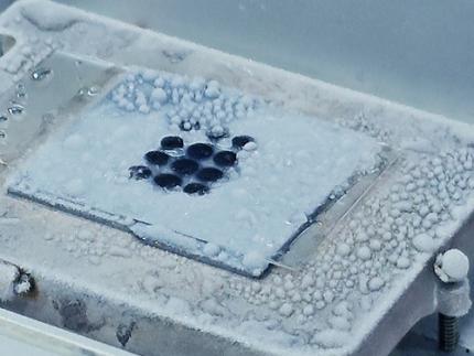 KAIST Research team develops anti-icing film that only requires sunlight
A KAIST research team has developed an anti-icing and de-icing film coating technology that can apply the photothermal effect of gold nanoparticles to industrial sites without the need for heating wires, periodic spray or oil coating of anti-freeze substances, and substrate design alterations.
The group led by Professor Hyoungsoo Kim from the Department of Mechanical Engineering (Fluid & Interface Laboratory) and Professor Dong Ki Yoon from the Department of Chemistry (Soft Material Assembly Group) revealed on January 3 to have together developed an original technique that can uniformly pattern gold nanorod (GNR) particles in quadrants through simple evaporation, and have used this to develop an anti-icing and de-icing surface.
Many scientists in recent years have tried to control substrate surfaces through various coating techniques, and those involving the patterning of functional nanomaterials have gained special attention. In particular, GNR is considered a promising candidate nanomaterial for its biocompatibility, chemical stability, relatively simple synthesis, and its stable and unique property of surface plasmon resonance. To maximize the performance of GNR, it is important to achieve a high uniformity during film deposition, and a high level of rod alignment. However, achieving both criteria has thus far been a difficult challenge.
< Figure 1. Conceptual image to display Hydrodynamic mechanisms for the formation of a homogeneous quadrant cellulose nanocrystal(CNC) matrix. >
To solve this, the joint research team utilized cellulose nanocrystal (CNC), a next-generation functional nanomaterial that can easily be extracted from nature. By co-assembling GNR on CNC quadrant templates, the team could uniformly dry the film and successfully obtain a GNR film with a uniform alignment in a ring-shape. Compared to existing coffee-ring films, the highly uniform and aligned GNR film developed through this research showed enhanced plasmonic photothermal properties, and the team showed that it could carry out anti-icing and de-icing functions by simply irradiating light in the visible wavelength range.
< Figure 2. Optical and thermal performance evaluation results of gold nanorod film and demonstration of plasmonic heater for anti-icing and de-icing. >
Professor Hyoungsoo Kim said, “This technique can be applied to plastic, as well as flexible surfaces. By using it on exterior materials and films, it can generate its own heat energy, which would greatly save energy through voluntary thermal energy harvesting across various applications including cars, aircrafts, and windows in residential or commercial spaces, where frosting becomes a serious issue in the winter.” Professor Dong Ki Yoon added, “This research is significant in that we can now freely pattern the CNC-GNR composite, which was previously difficult to create into films, over a large area. We can utilize this as an anti-icing material, and if we were to take advantage of the plasmonic properties of gold, we can also use it like stained-glass to decorate glass surfaces.”
This research was conducted by Ph.D. candidate Jeongsu Pyeon from the Department of Mechanical Engineering, and his co-first author Dr. Soon Mo Park (a KAIST graduate, currently a post-doctoral associate at Cornell University), and was pushed in the online volume of Nature Communication on December 8, 2023 under the title “Plasmonic Metasurfaces of Cellulose Nanocrystal Matrices with Quadrants of Aligned Gold Nanorods for Photothermal Anti-Icing." Recognized for its achievement, the research was also selected as an editor’s highlight for the journals Materials Science and Chemistry, and Inorganic and Physical Chemistry.
This research was supported by the Individual Basic Mid-Sized Research Fund from the National Research Foundation of Korea and the Center for Multiscale Chiral Architectures.
2024.01.16 View 4667
KAIST Research team develops anti-icing film that only requires sunlight
A KAIST research team has developed an anti-icing and de-icing film coating technology that can apply the photothermal effect of gold nanoparticles to industrial sites without the need for heating wires, periodic spray or oil coating of anti-freeze substances, and substrate design alterations.
The group led by Professor Hyoungsoo Kim from the Department of Mechanical Engineering (Fluid & Interface Laboratory) and Professor Dong Ki Yoon from the Department of Chemistry (Soft Material Assembly Group) revealed on January 3 to have together developed an original technique that can uniformly pattern gold nanorod (GNR) particles in quadrants through simple evaporation, and have used this to develop an anti-icing and de-icing surface.
Many scientists in recent years have tried to control substrate surfaces through various coating techniques, and those involving the patterning of functional nanomaterials have gained special attention. In particular, GNR is considered a promising candidate nanomaterial for its biocompatibility, chemical stability, relatively simple synthesis, and its stable and unique property of surface plasmon resonance. To maximize the performance of GNR, it is important to achieve a high uniformity during film deposition, and a high level of rod alignment. However, achieving both criteria has thus far been a difficult challenge.
< Figure 1. Conceptual image to display Hydrodynamic mechanisms for the formation of a homogeneous quadrant cellulose nanocrystal(CNC) matrix. >
To solve this, the joint research team utilized cellulose nanocrystal (CNC), a next-generation functional nanomaterial that can easily be extracted from nature. By co-assembling GNR on CNC quadrant templates, the team could uniformly dry the film and successfully obtain a GNR film with a uniform alignment in a ring-shape. Compared to existing coffee-ring films, the highly uniform and aligned GNR film developed through this research showed enhanced plasmonic photothermal properties, and the team showed that it could carry out anti-icing and de-icing functions by simply irradiating light in the visible wavelength range.
< Figure 2. Optical and thermal performance evaluation results of gold nanorod film and demonstration of plasmonic heater for anti-icing and de-icing. >
Professor Hyoungsoo Kim said, “This technique can be applied to plastic, as well as flexible surfaces. By using it on exterior materials and films, it can generate its own heat energy, which would greatly save energy through voluntary thermal energy harvesting across various applications including cars, aircrafts, and windows in residential or commercial spaces, where frosting becomes a serious issue in the winter.” Professor Dong Ki Yoon added, “This research is significant in that we can now freely pattern the CNC-GNR composite, which was previously difficult to create into films, over a large area. We can utilize this as an anti-icing material, and if we were to take advantage of the plasmonic properties of gold, we can also use it like stained-glass to decorate glass surfaces.”
This research was conducted by Ph.D. candidate Jeongsu Pyeon from the Department of Mechanical Engineering, and his co-first author Dr. Soon Mo Park (a KAIST graduate, currently a post-doctoral associate at Cornell University), and was pushed in the online volume of Nature Communication on December 8, 2023 under the title “Plasmonic Metasurfaces of Cellulose Nanocrystal Matrices with Quadrants of Aligned Gold Nanorods for Photothermal Anti-Icing." Recognized for its achievement, the research was also selected as an editor’s highlight for the journals Materials Science and Chemistry, and Inorganic and Physical Chemistry.
This research was supported by the Individual Basic Mid-Sized Research Fund from the National Research Foundation of Korea and the Center for Multiscale Chiral Architectures.
2024.01.16 View 4667 -
 KAIST develops an artificial muscle device that produces force 34 times its weight
- Professor IlKwon Oh’s research team in KAIST’s Department of Mechanical Engineering developed a soft fluidic switch using an ionic polymer artificial muscle that runs with ultra-low power to lift objects 34 times greater than its weight.
- Its light weight and small size make it applicable to various industrial fields such as soft electronics, smart textiles, and biomedical devices by controlling fluid flow with high precision, even in narrow spaces.
Soft robots, medical devices, and wearable devices have permeated our daily lives. KAIST researchers have developed a fluid switch using ionic polymer artificial muscles that operates at ultra-low power and produces a force 34 times greater than its weight. Fluid switches control fluid flow, causing the fluid to flow in a specific direction to invoke various movements.
KAIST (President Kwang-Hyung Lee) announced on the 4th of January that a research team under Professor IlKwon Oh from the Department of Mechanical Engineering has developed a soft fluidic switch that operates at ultra-low voltage and can be used in narrow spaces.
Artificial muscles imitate human muscles and provide flexible and natural movements compared to traditional motors, making them one of the basic elements used in soft robots, medical devices, and wearable devices. These artificial muscles create movements in response to external stimuli such as electricity, air pressure, and temperature changes, and in order to utilize artificial muscles, it is important to control these movements precisely.
Switches based on existing motors were difficult to use within limited spaces due to their rigidity and large size. In order to address these issues, the research team developed an electro-ionic soft actuator that can control fluid flow while producing large amounts of force, even in a narrow pipe, and used it as a soft fluidic switch.
< Figure 1. The separation of fluid droplets using a soft fluid switch at ultra-low voltage. >
The ionic polymer artificial muscle developed by the research team is composed of metal electrodes and ionic polymers, and it generates force and movement in response to electricity. A polysulfonated covalent organic framework (pS-COF) made by combining organic molecules on the surface of the artificial muscle electrode was used to generate an impressive amount of force relative to its weight with ultra-low power (~0.01V).
As a result, the artificial muscle, which was manufactured to be as thin as a hair with a thickness of 180 µm, produced a force more than 34 times greater than its light weight of 10 mg to initiate smooth movement. Through this, the research team was able to precisely control the direction of fluid flow with low power.
< Figure 2. The synthesis and use of pS-COF as a common electrode-electrolyte host for electroactive soft fluid switches. A) The synthesis schematic of pS-COF. B) The schematic diagram of the operating principle of the electrochemical soft switch. C) The schematic diagram of using a pS-COF-based electrochemical soft switch to control fluid flow in dynamic operation. >
Professor IlKwon Oh, who led this research, said, “The electrochemical soft fluidic switch that operate at ultra-low power can open up many possibilities in the fields of soft robots, soft electronics, and microfluidics based on fluid control.” He added, “From smart fibers to biomedical devices, this technology has the potential to be immediately put to use in a variety of industrial settings as it can be easily applied to ultra-small electronic systems in our daily lives.”
The results of this study, in which Dr. Manmatha Mahato, a research professor in the Department of Mechanical Engineering at KAIST, participated as the first author, were published in the international academic journal Science Advances on December 13, 2023. (Paper title: Polysulfonated Covalent Organic Framework as Active Electrode Host for Mobile Cation Guests in Electrochemical Soft Actuator)
This research was conducted with support from the National Research Foundation of Korea's Leader Scientist Support Project (Creative Research Group) and Future Convergence Pioneer Project.
* Paper DOI: https://www.science.org/doi/abs/10.1126/sciadv.adk9752
2024.01.11 View 4428
KAIST develops an artificial muscle device that produces force 34 times its weight
- Professor IlKwon Oh’s research team in KAIST’s Department of Mechanical Engineering developed a soft fluidic switch using an ionic polymer artificial muscle that runs with ultra-low power to lift objects 34 times greater than its weight.
- Its light weight and small size make it applicable to various industrial fields such as soft electronics, smart textiles, and biomedical devices by controlling fluid flow with high precision, even in narrow spaces.
Soft robots, medical devices, and wearable devices have permeated our daily lives. KAIST researchers have developed a fluid switch using ionic polymer artificial muscles that operates at ultra-low power and produces a force 34 times greater than its weight. Fluid switches control fluid flow, causing the fluid to flow in a specific direction to invoke various movements.
KAIST (President Kwang-Hyung Lee) announced on the 4th of January that a research team under Professor IlKwon Oh from the Department of Mechanical Engineering has developed a soft fluidic switch that operates at ultra-low voltage and can be used in narrow spaces.
Artificial muscles imitate human muscles and provide flexible and natural movements compared to traditional motors, making them one of the basic elements used in soft robots, medical devices, and wearable devices. These artificial muscles create movements in response to external stimuli such as electricity, air pressure, and temperature changes, and in order to utilize artificial muscles, it is important to control these movements precisely.
Switches based on existing motors were difficult to use within limited spaces due to their rigidity and large size. In order to address these issues, the research team developed an electro-ionic soft actuator that can control fluid flow while producing large amounts of force, even in a narrow pipe, and used it as a soft fluidic switch.
< Figure 1. The separation of fluid droplets using a soft fluid switch at ultra-low voltage. >
The ionic polymer artificial muscle developed by the research team is composed of metal electrodes and ionic polymers, and it generates force and movement in response to electricity. A polysulfonated covalent organic framework (pS-COF) made by combining organic molecules on the surface of the artificial muscle electrode was used to generate an impressive amount of force relative to its weight with ultra-low power (~0.01V).
As a result, the artificial muscle, which was manufactured to be as thin as a hair with a thickness of 180 µm, produced a force more than 34 times greater than its light weight of 10 mg to initiate smooth movement. Through this, the research team was able to precisely control the direction of fluid flow with low power.
< Figure 2. The synthesis and use of pS-COF as a common electrode-electrolyte host for electroactive soft fluid switches. A) The synthesis schematic of pS-COF. B) The schematic diagram of the operating principle of the electrochemical soft switch. C) The schematic diagram of using a pS-COF-based electrochemical soft switch to control fluid flow in dynamic operation. >
Professor IlKwon Oh, who led this research, said, “The electrochemical soft fluidic switch that operate at ultra-low power can open up many possibilities in the fields of soft robots, soft electronics, and microfluidics based on fluid control.” He added, “From smart fibers to biomedical devices, this technology has the potential to be immediately put to use in a variety of industrial settings as it can be easily applied to ultra-small electronic systems in our daily lives.”
The results of this study, in which Dr. Manmatha Mahato, a research professor in the Department of Mechanical Engineering at KAIST, participated as the first author, were published in the international academic journal Science Advances on December 13, 2023. (Paper title: Polysulfonated Covalent Organic Framework as Active Electrode Host for Mobile Cation Guests in Electrochemical Soft Actuator)
This research was conducted with support from the National Research Foundation of Korea's Leader Scientist Support Project (Creative Research Group) and Future Convergence Pioneer Project.
* Paper DOI: https://www.science.org/doi/abs/10.1126/sciadv.adk9752
2024.01.11 View 4428 -
 KAIST Demonstrates AI and sustainable technologies at CES 2024
On January 2, KAIST announced it will be participating in the Consumer Electronics Show (CES) 2024, held between January 9 and 12.
CES 2024 is one of the world’s largest tech conferences to take place in Las Vegas. Under the slogan “KAIST, the Global Value Creator” for its exhibition, KAIST has submitted technologies falling under one of following themes: “Expansion of Human Intelligence, Mobility, and Reality”, and “Pursuit of Human Security and Sustainable Development”.
24 startups and pre-startups whose technologies stand out in various fields including artificial intelligence (AI), mobility, virtual reality, healthcare and human security, and sustainable development, will welcome their visitors at an exclusive booth of 232 m2 prepared for KAIST at Eureka Park in Las Vegas.
12 businesses will participate in the first category, “Expansion of Human Intelligence, Mobility, and Reality”, including MicroPix, Panmnesia, DeepAuto, MGL, Reports, Narnia Labs, EL FACTORY, Korea Position Technology, AudAi, Planby Technologies, Movin, and Studio Lab.
In the “Pursuit of Human Security and Sustainable Development” category, 12 businesses including Aldaver, ADNC, Solve, Iris, Blue Device, Barreleye, TR, A2US, Greeners, Iron Boys, Shard Partners and Kingbot, will be introduced.
In particular, Aldaver is a startup that received the Korean Business Award 2023 as well as the presidential award at the Challenge K-Startup with its biomimetic material and printing technology. It has attracted 4.5 billion KRW of investment thus far.
Narnia Labs, with its AI design solution for manufacturing, won the grand prize for K-tech Startups 2022, and has so far attracted 3.5 billion KRW of investments.
Panmnesia is a startup that won the 2024 CES Innovation Award, recognized for their fab-less AI semiconductor technology. They attracted 16 billion KRW of investment through seed round alone.
Meanwhile, student startups will also be presented during the exhibition. Studio Lab received a CES 2024 Best of Innovation Award in the AI category. The team developed the software Seller Canvas, which automatically generates a page for product details when a user uploads an image of a product.
The central stage at the KAIST exhibition booth will be used to interview members of the participating startups between Jan 9 to 11, as well as a networking site for businesses and invited investors during KAIST NIGHT on the evening of 10th, between 5 and 7 PM.
Director Sung-Yool Choi of the KAIST Institute of Technology Value Creation said, “Through CES 2024, KAIST will overcome the limits of human intelligence, mobility, and space with the deep-tech based technologies developed by its startups, and will demonstrate its achievements for realizing its vision as a global value-creating university through the solutions for human security and sustainable development.”
2024.01.05 View 3342
KAIST Demonstrates AI and sustainable technologies at CES 2024
On January 2, KAIST announced it will be participating in the Consumer Electronics Show (CES) 2024, held between January 9 and 12.
CES 2024 is one of the world’s largest tech conferences to take place in Las Vegas. Under the slogan “KAIST, the Global Value Creator” for its exhibition, KAIST has submitted technologies falling under one of following themes: “Expansion of Human Intelligence, Mobility, and Reality”, and “Pursuit of Human Security and Sustainable Development”.
24 startups and pre-startups whose technologies stand out in various fields including artificial intelligence (AI), mobility, virtual reality, healthcare and human security, and sustainable development, will welcome their visitors at an exclusive booth of 232 m2 prepared for KAIST at Eureka Park in Las Vegas.
12 businesses will participate in the first category, “Expansion of Human Intelligence, Mobility, and Reality”, including MicroPix, Panmnesia, DeepAuto, MGL, Reports, Narnia Labs, EL FACTORY, Korea Position Technology, AudAi, Planby Technologies, Movin, and Studio Lab.
In the “Pursuit of Human Security and Sustainable Development” category, 12 businesses including Aldaver, ADNC, Solve, Iris, Blue Device, Barreleye, TR, A2US, Greeners, Iron Boys, Shard Partners and Kingbot, will be introduced.
In particular, Aldaver is a startup that received the Korean Business Award 2023 as well as the presidential award at the Challenge K-Startup with its biomimetic material and printing technology. It has attracted 4.5 billion KRW of investment thus far.
Narnia Labs, with its AI design solution for manufacturing, won the grand prize for K-tech Startups 2022, and has so far attracted 3.5 billion KRW of investments.
Panmnesia is a startup that won the 2024 CES Innovation Award, recognized for their fab-less AI semiconductor technology. They attracted 16 billion KRW of investment through seed round alone.
Meanwhile, student startups will also be presented during the exhibition. Studio Lab received a CES 2024 Best of Innovation Award in the AI category. The team developed the software Seller Canvas, which automatically generates a page for product details when a user uploads an image of a product.
The central stage at the KAIST exhibition booth will be used to interview members of the participating startups between Jan 9 to 11, as well as a networking site for businesses and invited investors during KAIST NIGHT on the evening of 10th, between 5 and 7 PM.
Director Sung-Yool Choi of the KAIST Institute of Technology Value Creation said, “Through CES 2024, KAIST will overcome the limits of human intelligence, mobility, and space with the deep-tech based technologies developed by its startups, and will demonstrate its achievements for realizing its vision as a global value-creating university through the solutions for human security and sustainable development.”
2024.01.05 View 3342 -
 A KAIST Research Team Develops High-Performance Stretchable Solar Cells
With the market for wearable electric devices growing rapidly, stretchable solar cells that can function under strain have received considerable attention as an energy source. To build such solar cells, it is necessary that their photoactive layer, which converts light into electricity, shows high electrical performance while possessing mechanical elasticity. However, satisfying both of these two requirements is challenging, making stretchable solar cells difficult to develop.
On December 26, a KAIST research team from the Department of Chemical and Biomolecular Engineering (CBE) led by Professor Bumjoon Kim announced the development of a new conductive polymer material that achieved both high electrical performance and elasticity while introducing the world’s highest-performing stretchable organic solar cell.
Organic solar cells are devices whose photoactive layer, which is responsible for the conversion of light into electricity, is composed of organic materials. Compared to existing non-organic material-based solar cells, they are lighter and flexible, making them highly applicable for wearable electrical devices. Solar cells as an energy source are particularly important for building electrical devices, but high-efficiency solar cells often lack flexibility, and their application in wearable devices have therefore been limited to this point.
The team led by Professor Kim conjugated a highly stretchable polymer to an electrically conductive polymer with excellent electrical properties through chemical bonding, and developed a new conductive polymer with both electrical conductivity and mechanical stretchability. This polymer meets the highest reported level of photovoltaic conversion efficiency (19%) using organic solar cells, while also showing 10 times the stretchability of existing devices. The team thereby built the world’s highest performing stretchable solar cell that can be stretched up to 40% during operation, and demonstrated its applicability for wearable devices.
< Figure 1. Chemical structure of the newly developed conductive polymer and performance of stretchable organic solar cells using the material. >
Professor Kim said, “Through this research, we not only developed the world’s best performing stretchable organic solar cell, but it is also significant that we developed a new polymer that can be applicable as a base material for various electronic devices that needs to be malleable and/or elastic.”
< Figure 2. Photovoltaic efficiency and mechanical stretchability of newly developed polymers compared to existing polymers. >
This research, conducted by KAIST researchers Jin-Woo Lee and Heung-Goo Lee as first co-authors in cooperation with teams led by Professor Taek-Soo Kim from the Department of Mechanical Engineering and Professor Sheng Li from the Department of CBE, was published in Joule on December 1 (Paper Title: Rigid and Soft Block-Copolymerized Conjugated Polymers Enable High-Performance Intrinsically-Stretchable Organic Solar Cells).
This research was supported by the National Research Foundation of Korea.
2024.01.04 View 3455
A KAIST Research Team Develops High-Performance Stretchable Solar Cells
With the market for wearable electric devices growing rapidly, stretchable solar cells that can function under strain have received considerable attention as an energy source. To build such solar cells, it is necessary that their photoactive layer, which converts light into electricity, shows high electrical performance while possessing mechanical elasticity. However, satisfying both of these two requirements is challenging, making stretchable solar cells difficult to develop.
On December 26, a KAIST research team from the Department of Chemical and Biomolecular Engineering (CBE) led by Professor Bumjoon Kim announced the development of a new conductive polymer material that achieved both high electrical performance and elasticity while introducing the world’s highest-performing stretchable organic solar cell.
Organic solar cells are devices whose photoactive layer, which is responsible for the conversion of light into electricity, is composed of organic materials. Compared to existing non-organic material-based solar cells, they are lighter and flexible, making them highly applicable for wearable electrical devices. Solar cells as an energy source are particularly important for building electrical devices, but high-efficiency solar cells often lack flexibility, and their application in wearable devices have therefore been limited to this point.
The team led by Professor Kim conjugated a highly stretchable polymer to an electrically conductive polymer with excellent electrical properties through chemical bonding, and developed a new conductive polymer with both electrical conductivity and mechanical stretchability. This polymer meets the highest reported level of photovoltaic conversion efficiency (19%) using organic solar cells, while also showing 10 times the stretchability of existing devices. The team thereby built the world’s highest performing stretchable solar cell that can be stretched up to 40% during operation, and demonstrated its applicability for wearable devices.
< Figure 1. Chemical structure of the newly developed conductive polymer and performance of stretchable organic solar cells using the material. >
Professor Kim said, “Through this research, we not only developed the world’s best performing stretchable organic solar cell, but it is also significant that we developed a new polymer that can be applicable as a base material for various electronic devices that needs to be malleable and/or elastic.”
< Figure 2. Photovoltaic efficiency and mechanical stretchability of newly developed polymers compared to existing polymers. >
This research, conducted by KAIST researchers Jin-Woo Lee and Heung-Goo Lee as first co-authors in cooperation with teams led by Professor Taek-Soo Kim from the Department of Mechanical Engineering and Professor Sheng Li from the Department of CBE, was published in Joule on December 1 (Paper Title: Rigid and Soft Block-Copolymerized Conjugated Polymers Enable High-Performance Intrinsically-Stretchable Organic Solar Cells).
This research was supported by the National Research Foundation of Korea.
2024.01.04 View 3455 -
 KAIST presents strategies for environmentally friendly and sustainable polyamides production
- Provides current research trends in bio-based polyamide production
- Research on bio-based polyamides production gains importance for achieving a carbon-neutral society
Global industries focused on carbon neutrality, under the slogan "Net-Zero," are gaining increasing attention. In particular, research on microbial production of polymers, replacing traditional chemical methods with biological approaches, is actively progressing.
Polyamides, represented by nylon, are linear polymers widely used in various industries such as automotive, electronics, textiles, and medical fields. They possess beneficial properties such as high tensile strength, electrical insulation, heat resistance, wear resistance, and biocompatibility. Since the commercialization of nylon in 1938, approximately 7 million tons of polyamides are produced worldwide annually. Considering their broad applications and significance, producing polyamides through bio-based methods holds considerable environmental and industrial importance.
KAIST (President Kwang-Hyung Lee) announced that a research team led by Distinguished Professor Sang Yup Lee, including Dr. Jong An Lee and doctoral candidate Ji Yeon Kim from the Department of Chemical and Biomolecular Engineering, published a paper titled "Current Advancements in Bio-Based Production of Polyamides”. The paper was featured on the cover of the monthly issue of "Trends in Chemistry” by Cell Press.
As part of climate change response technologies, bio-refineries involve using biotechnological and chemical methods to produce industrially important chemicals and biofuels from renewable biomass without relying on fossil resources. Notably, systems metabolic engineering, pioneered by KAIST's Distinguished Professor Sang Yup Lee, is a research field that effectively manipulates microbial metabolic pathways to produce valuable chemicals, forming the core technology for bio-refineries. The research team has successfully developed high-performance strains producing a variety of compounds, including succinic acid, biodegradable plastics, biofuels, and natural products, using systems metabolic engineering tools and strategies.
The research team predicted that if bio-based polyamide production technology, which is widely used in the production of clothing and textiles, becomes widespread, it will attract attention as a future technology that can respond to the climate crisis due to its environment-friendly production technology. In this study, the research team comprehensively reviewed the bio-based polyamide production strategies. They provided insights into the advancements in polyamide monomer production using metabolically engineered microorganisms and highlighted the recent trends in bio-based polyamide advancements utilizing these monomers. Additionally, they reviewed the strategies for synthesizing bio-based polyamides through chemical conversion of natural oils and discussed the biodegradability and recycling of the polyamides. Furthermore, the paper presented the future direction in which metabolic engineering can be applied for the bio-based polyamide production, contributing to environmentally friendly and sustainable society.
Ji Yeon Kim, the co-first author of this paper from KAIST, stated "The importance of utilizing systems metabolic engineering tools and strategies for bio-based polyamides production is becoming increasingly prominent in achieving carbon neutrality."
Professor Sang Yup Lee emphasized, "Amid growing concerns about climate change, the significance of environmentally friendly and sustainable industrial development is greater than ever. Systems metabolic engineering is expected to have a significant impact not only on the chemical industry but also in various fields."
< [Figure 1] A schematic overview of the overall process for polyamides production >
This paper by Dr. Jong An Lee, PhD student Ji Yeon Kim, Dr. Jung Ho Ahn, and Master Yeah-Ji Ahn from the Department of Chemical and Biomolecular Engineering at KAIST was published in the December issue of 'Trends in Chemistry', an authoritative review journal in the field of chemistry published by Cell. It was published on December 7 as the cover paper and featured review.
※ Paper title: Current advancements in the bio-based production of polyamides
※ Author information: Jong An Lee, Ji Yeon Kim, Jung Ho Ahn, Yeah-Ji Ahn, and Sang Yup Lee
This research was conducted with the support from the development of platform technologies of microbial cell factories for the next-generation biorefineries project and C1 gas refinery program by Korean Ministry of Science and ICT.
< [Figure 2] Cover paper of the December issue of Trends in Chemistry >
2023.12.21 View 2338
KAIST presents strategies for environmentally friendly and sustainable polyamides production
- Provides current research trends in bio-based polyamide production
- Research on bio-based polyamides production gains importance for achieving a carbon-neutral society
Global industries focused on carbon neutrality, under the slogan "Net-Zero," are gaining increasing attention. In particular, research on microbial production of polymers, replacing traditional chemical methods with biological approaches, is actively progressing.
Polyamides, represented by nylon, are linear polymers widely used in various industries such as automotive, electronics, textiles, and medical fields. They possess beneficial properties such as high tensile strength, electrical insulation, heat resistance, wear resistance, and biocompatibility. Since the commercialization of nylon in 1938, approximately 7 million tons of polyamides are produced worldwide annually. Considering their broad applications and significance, producing polyamides through bio-based methods holds considerable environmental and industrial importance.
KAIST (President Kwang-Hyung Lee) announced that a research team led by Distinguished Professor Sang Yup Lee, including Dr. Jong An Lee and doctoral candidate Ji Yeon Kim from the Department of Chemical and Biomolecular Engineering, published a paper titled "Current Advancements in Bio-Based Production of Polyamides”. The paper was featured on the cover of the monthly issue of "Trends in Chemistry” by Cell Press.
As part of climate change response technologies, bio-refineries involve using biotechnological and chemical methods to produce industrially important chemicals and biofuels from renewable biomass without relying on fossil resources. Notably, systems metabolic engineering, pioneered by KAIST's Distinguished Professor Sang Yup Lee, is a research field that effectively manipulates microbial metabolic pathways to produce valuable chemicals, forming the core technology for bio-refineries. The research team has successfully developed high-performance strains producing a variety of compounds, including succinic acid, biodegradable plastics, biofuels, and natural products, using systems metabolic engineering tools and strategies.
The research team predicted that if bio-based polyamide production technology, which is widely used in the production of clothing and textiles, becomes widespread, it will attract attention as a future technology that can respond to the climate crisis due to its environment-friendly production technology. In this study, the research team comprehensively reviewed the bio-based polyamide production strategies. They provided insights into the advancements in polyamide monomer production using metabolically engineered microorganisms and highlighted the recent trends in bio-based polyamide advancements utilizing these monomers. Additionally, they reviewed the strategies for synthesizing bio-based polyamides through chemical conversion of natural oils and discussed the biodegradability and recycling of the polyamides. Furthermore, the paper presented the future direction in which metabolic engineering can be applied for the bio-based polyamide production, contributing to environmentally friendly and sustainable society.
Ji Yeon Kim, the co-first author of this paper from KAIST, stated "The importance of utilizing systems metabolic engineering tools and strategies for bio-based polyamides production is becoming increasingly prominent in achieving carbon neutrality."
Professor Sang Yup Lee emphasized, "Amid growing concerns about climate change, the significance of environmentally friendly and sustainable industrial development is greater than ever. Systems metabolic engineering is expected to have a significant impact not only on the chemical industry but also in various fields."
< [Figure 1] A schematic overview of the overall process for polyamides production >
This paper by Dr. Jong An Lee, PhD student Ji Yeon Kim, Dr. Jung Ho Ahn, and Master Yeah-Ji Ahn from the Department of Chemical and Biomolecular Engineering at KAIST was published in the December issue of 'Trends in Chemistry', an authoritative review journal in the field of chemistry published by Cell. It was published on December 7 as the cover paper and featured review.
※ Paper title: Current advancements in the bio-based production of polyamides
※ Author information: Jong An Lee, Ji Yeon Kim, Jung Ho Ahn, Yeah-Ji Ahn, and Sang Yup Lee
This research was conducted with the support from the development of platform technologies of microbial cell factories for the next-generation biorefineries project and C1 gas refinery program by Korean Ministry of Science and ICT.
< [Figure 2] Cover paper of the December issue of Trends in Chemistry >
2023.12.21 View 2338 -
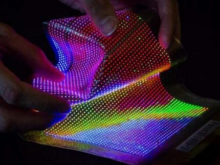 A KAIST Team Develops Selective Transfer Printing Technology for MicroLEDs
- A KAIST research team led by Professor Keon Jae Lee demonstrates the transfer printing of a large number of micro-sized inorganic semiconductor chips via the selective modulation of micro-vacuum force.
MicroLEDs are a light source for next-generation displays that utilize inorganic LED chips with a size of less than 100 μm. MicroLEDs have attracted a great deal of attention due to their superior electrical/optical properties, reliability, and stability compared to conventional displays such as LCD, OLED, and QD. To commercialize microLEDs, transfer printing technology is essential for rearranging microLED dies from a growth substrate onto the final substrate with a desired layout and precise alignment. However, previous transfer methods still have many challenges such as the need for additional adhesives, misalignment, low transfer yield, and chip damage.
Professor Lee’s research team has developed a micro-vacuum assisted selective transfer printing (µVAST) technology to transfer a large number of microLED chips by adjusting the micro-vacuum suction force.
The key technology relies on a laser-induced etching (LIE) method for forming 20 μm-sized micro-hole arrays with a high aspect ratio on glass substrates at fabrication speed of up to 7,000 holes per second. The LIE-drilled glass is connected to the vacuum channels, controlling the micro-vacuum force at desired hole arrays to selectively pick up and release the microLEDs. The micro-vacuum assisted transfer printing accomplishes a higher adhesion switchability compared to previous transfer methods, enabling the assembly of micro-sized semiconductors with various heterogeneous materials, sizes, shapes, and thicknesses onto arbitrary substrates with high transfer yields.
< Figure 01. Concept of micro-vacuum assisted selective transfer printing (μVAST). >
Professor Keon Jae Lee said, “The micro-vacuum assisted transfer provides an interesting tool for large-scale, selective integration of microscale high-performance inorganic semiconductors. Currently, we are investigating the transfer printing of commercial microLED chips with an ejector system for commercializing next-generation displays (Large screen TVs, flexible/stretchable devices) and wearable phototherapy patches.”
This result titled “Universal selective transfer printing via micro-vacuum force” was published in Nature Communications on November 26th, 2023. (DOI: 10.1038/S41467-023-43342-8)
< Figure 02. Universal transfer printing of thin-film semiconductors via μVAST. >
< Figure 03. Flexible devices fabricated by μVAST. >
Title: Entire process including LIE and µVAST
Vimeo link: https://vimeo.com/894430416?share=copy
2023.12.19 View 1618
A KAIST Team Develops Selective Transfer Printing Technology for MicroLEDs
- A KAIST research team led by Professor Keon Jae Lee demonstrates the transfer printing of a large number of micro-sized inorganic semiconductor chips via the selective modulation of micro-vacuum force.
MicroLEDs are a light source for next-generation displays that utilize inorganic LED chips with a size of less than 100 μm. MicroLEDs have attracted a great deal of attention due to their superior electrical/optical properties, reliability, and stability compared to conventional displays such as LCD, OLED, and QD. To commercialize microLEDs, transfer printing technology is essential for rearranging microLED dies from a growth substrate onto the final substrate with a desired layout and precise alignment. However, previous transfer methods still have many challenges such as the need for additional adhesives, misalignment, low transfer yield, and chip damage.
Professor Lee’s research team has developed a micro-vacuum assisted selective transfer printing (µVAST) technology to transfer a large number of microLED chips by adjusting the micro-vacuum suction force.
The key technology relies on a laser-induced etching (LIE) method for forming 20 μm-sized micro-hole arrays with a high aspect ratio on glass substrates at fabrication speed of up to 7,000 holes per second. The LIE-drilled glass is connected to the vacuum channels, controlling the micro-vacuum force at desired hole arrays to selectively pick up and release the microLEDs. The micro-vacuum assisted transfer printing accomplishes a higher adhesion switchability compared to previous transfer methods, enabling the assembly of micro-sized semiconductors with various heterogeneous materials, sizes, shapes, and thicknesses onto arbitrary substrates with high transfer yields.
< Figure 01. Concept of micro-vacuum assisted selective transfer printing (μVAST). >
Professor Keon Jae Lee said, “The micro-vacuum assisted transfer provides an interesting tool for large-scale, selective integration of microscale high-performance inorganic semiconductors. Currently, we are investigating the transfer printing of commercial microLED chips with an ejector system for commercializing next-generation displays (Large screen TVs, flexible/stretchable devices) and wearable phototherapy patches.”
This result titled “Universal selective transfer printing via micro-vacuum force” was published in Nature Communications on November 26th, 2023. (DOI: 10.1038/S41467-023-43342-8)
< Figure 02. Universal transfer printing of thin-film semiconductors via μVAST. >
< Figure 03. Flexible devices fabricated by μVAST. >
Title: Entire process including LIE and µVAST
Vimeo link: https://vimeo.com/894430416?share=copy
2023.12.19 View 1618