School+of+Electrical+Engineering
-
 An Improved Carbon Nanotube Semiconductor
Professor Yang-Kyu Choi and his research team of the School of Electrical Engineering at KAIST collaborated with Professor Sung-Jin Choi of Kookmin University to develop a large-scale carbon nanotube semiconductor by using a 3-D fin-gate structure with carbon nanotubes on its top.
Dong Il Lee, a postdoctoral researcher at KAIST’s Electrical Engineering School, participated in this study as the first author. It was published in ACS Nano on November 10, 2016, and was entitled “Three-Dimensional Fin-Structured Semiconducting Carbon Nanotube Network Transistor.”
A semiconductor made with carbon nanotubes operates faster than a silicon semiconductor and requires less energy, yielding higher performance.
Most electronic equipment and devices, however, use silicon semiconductors because it is difficult to fabricate highly purified and densely packed semiconductors with carbon nanotubes (CNTs).
To date, the performance of CNTs was limited due to their low density. Their purity was also low, so it was impossible to make products that had a constant yield on a large-surface wafer or substrate. These characteristics made the mass production of semiconducting CNTs difficult.
To solve these difficulties, the research team used a 3-D fin-gate to vapor-deposit carbon nanotubes on its top. They developed a semiconductor that had a high current density with a width less than 50 nm.
The three-dimensional fin structure was able to vapor-deposit 600 carbon nanotubes per micrometer. This structure could have 20 times more nanotubes than the two dimensional structure, which could only vapor-deposit thirty in the same 1 micrometer width.
In addition, the research team used semi-conductive carbon nanotubes having a purity rating higher than 99.9% from a previous study to obtain a high yield semiconductor.
The semiconductor from the research group has a high current density even with a width less than 50 μm. The new semiconductor is expected to be five times faster than a silicon-based semiconductor and will require five times less electricity during operation.
Furthermore, the new semiconductor can be made by or will be compatible with the equipment for producing silicon-based semiconductors, so there will be no additional costs.
Researcher Lee said, “As a next generation semiconductor, the carbon nanotube semiconductor will have better performance, and its effectiveness will be higher.” He also added, “Hopefully, the new semiconductor will replace the silicon-based semiconductors in ten years.”
This study received support from the Center for Integrated Smart Sensors funded by the Ministry of Science, ICT & Future Planning of Korea as the Global Frontier Project, and from the CMOS (Complementary Metal-Oxide-Semiconductor) THz Technology Convergence Center of the Pioneer Research Center Program sponsored by the National Research Foundation of Korea.
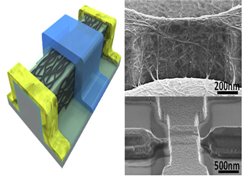
Picture 1: 3D Diagram of the Carbon Nanotube Electronic Device and Its Scanning Electron Microscope (SEM) Image
Picture 2: 3D Transistor Device on an 8-inch Base and the SEM Image of Its Cross Section
2017.02.16 View 8586
An Improved Carbon Nanotube Semiconductor
Professor Yang-Kyu Choi and his research team of the School of Electrical Engineering at KAIST collaborated with Professor Sung-Jin Choi of Kookmin University to develop a large-scale carbon nanotube semiconductor by using a 3-D fin-gate structure with carbon nanotubes on its top.
Dong Il Lee, a postdoctoral researcher at KAIST’s Electrical Engineering School, participated in this study as the first author. It was published in ACS Nano on November 10, 2016, and was entitled “Three-Dimensional Fin-Structured Semiconducting Carbon Nanotube Network Transistor.”
A semiconductor made with carbon nanotubes operates faster than a silicon semiconductor and requires less energy, yielding higher performance.
Most electronic equipment and devices, however, use silicon semiconductors because it is difficult to fabricate highly purified and densely packed semiconductors with carbon nanotubes (CNTs).
To date, the performance of CNTs was limited due to their low density. Their purity was also low, so it was impossible to make products that had a constant yield on a large-surface wafer or substrate. These characteristics made the mass production of semiconducting CNTs difficult.
To solve these difficulties, the research team used a 3-D fin-gate to vapor-deposit carbon nanotubes on its top. They developed a semiconductor that had a high current density with a width less than 50 nm.
The three-dimensional fin structure was able to vapor-deposit 600 carbon nanotubes per micrometer. This structure could have 20 times more nanotubes than the two dimensional structure, which could only vapor-deposit thirty in the same 1 micrometer width.
In addition, the research team used semi-conductive carbon nanotubes having a purity rating higher than 99.9% from a previous study to obtain a high yield semiconductor.
The semiconductor from the research group has a high current density even with a width less than 50 μm. The new semiconductor is expected to be five times faster than a silicon-based semiconductor and will require five times less electricity during operation.
Furthermore, the new semiconductor can be made by or will be compatible with the equipment for producing silicon-based semiconductors, so there will be no additional costs.
Researcher Lee said, “As a next generation semiconductor, the carbon nanotube semiconductor will have better performance, and its effectiveness will be higher.” He also added, “Hopefully, the new semiconductor will replace the silicon-based semiconductors in ten years.”
This study received support from the Center for Integrated Smart Sensors funded by the Ministry of Science, ICT & Future Planning of Korea as the Global Frontier Project, and from the CMOS (Complementary Metal-Oxide-Semiconductor) THz Technology Convergence Center of the Pioneer Research Center Program sponsored by the National Research Foundation of Korea.
Picture 1: 3D Diagram of the Carbon Nanotube Electronic Device and Its Scanning Electron Microscope (SEM) Image
Picture 2: 3D Transistor Device on an 8-inch Base and the SEM Image of Its Cross Section
2017.02.16 View 8586 -
 Extremely Thin and Highly Flexible Graphene-Based Thermoacoustic Speakers
A joint research team led by Professors Jung-Woo Choi and Byung Jin Cho of the School of Electrical Engineering and Professor Sang Ouk Kim of the Material Science and Engineering Department, all on the faculty of the Korea Advanced Institute of Science and Technology (KAIST), has developed a simpler way to mass-produce ultra-thin graphene thermosacoustic speakers.
Their research results were published online on August 17, 2016 in a journal called Applied Materials & Interfaces. The IEEE Spectrum, a monthly magazine published by the Institute of Electrical and Electronics Engineers, reported on the research on September 9, 2016, in an article titled, “Graphene Enables Flat Speakers for Mobile Audio Systems.” The American Chemical Society also drew attention to the team’s work in its article dated September 7, 2016, “Bringing Graphene Speakers to the Mobile Market.”
Thermoacoustic speakers generate sound waves from temperature fluctuations by rapidly heating and cooling conducting materials. Unlike conventional voice-coil speakers, thermoacoustic speakers do not rely on vibrations to produce sound, and thus do not need bulky acoustic boxes to keep complicated mechanical parts for sound production. They also generate good quality sound in all directions, enabling them to be placed on any surface including curved ones without canceling out sounds generated from opposite sides.
Based on a two-step, template-free fabrication method that involved freeze-drying a solution of graphene oxide flakes and the reduction/doping of oxidized graphene to improve electrical properties, the research team produced a N-doped, three-dimensional (3D), reduced graphene oxide aerogel (N-rGOA) with a porous macroscopic structure that permitted easy modulation for many potential applications.
Using 3D graphene aerogels, the team succeeded in fabricating an array of loudspeakers that were able to withstand over 40 W input power and that showed excellent sound pressure level (SPL), comparable to those of previously reported 2D and 3D graphene loudspeakers.
Choong Sun Kim, the lead author of the research paper and a doctoral student in the School of Electrical Engineering at KAIST, said:
“Thermoacoustic speakers have a higher efficiency when conducting materials have a smaller heat capacity. Nanomaterials such as graphene are an ideal candidate for conductors, but they require a substrate to support their extremely thinness. The substrate’s tendency to lose heat lowers the speakers’ efficiency. Here, we developed 3D graphene aerogels without a substrate by using a simple two-step process. With graphene aerogels, we have fabricated an array of loudspeakers that demonstrated stable performance. This is a practical technology that will enable mass-production of thermosacoustic speakers including on mobile platforms.”
The research paper is entitled “Application of N-Doped Three-Dimensional Reduced Graphene Oxide Aerogel to Thin Film Loudspeaker.” (DOI: 10.1021/acsami.6b03618)
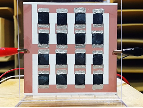
Figure 1: A Thermoacoustic Loudspeaker Consisted of an Array of 16 3D Graphene Aerogels
Figure 2: Two-step Fabrication Process of 3D Reduced Graphene Oxide Aerogel Using Freeze-Drying and Reduction/Doping
Figure 3: X-ray Photoelectron Spectroscopy Graph of the 3D Reduced Graphene Oxide Aerogel and Its Scanning Electron Microscope Image
2016.10.05 View 10637
Extremely Thin and Highly Flexible Graphene-Based Thermoacoustic Speakers
A joint research team led by Professors Jung-Woo Choi and Byung Jin Cho of the School of Electrical Engineering and Professor Sang Ouk Kim of the Material Science and Engineering Department, all on the faculty of the Korea Advanced Institute of Science and Technology (KAIST), has developed a simpler way to mass-produce ultra-thin graphene thermosacoustic speakers.
Their research results were published online on August 17, 2016 in a journal called Applied Materials & Interfaces. The IEEE Spectrum, a monthly magazine published by the Institute of Electrical and Electronics Engineers, reported on the research on September 9, 2016, in an article titled, “Graphene Enables Flat Speakers for Mobile Audio Systems.” The American Chemical Society also drew attention to the team’s work in its article dated September 7, 2016, “Bringing Graphene Speakers to the Mobile Market.”
Thermoacoustic speakers generate sound waves from temperature fluctuations by rapidly heating and cooling conducting materials. Unlike conventional voice-coil speakers, thermoacoustic speakers do not rely on vibrations to produce sound, and thus do not need bulky acoustic boxes to keep complicated mechanical parts for sound production. They also generate good quality sound in all directions, enabling them to be placed on any surface including curved ones without canceling out sounds generated from opposite sides.
Based on a two-step, template-free fabrication method that involved freeze-drying a solution of graphene oxide flakes and the reduction/doping of oxidized graphene to improve electrical properties, the research team produced a N-doped, three-dimensional (3D), reduced graphene oxide aerogel (N-rGOA) with a porous macroscopic structure that permitted easy modulation for many potential applications.
Using 3D graphene aerogels, the team succeeded in fabricating an array of loudspeakers that were able to withstand over 40 W input power and that showed excellent sound pressure level (SPL), comparable to those of previously reported 2D and 3D graphene loudspeakers.
Choong Sun Kim, the lead author of the research paper and a doctoral student in the School of Electrical Engineering at KAIST, said:
“Thermoacoustic speakers have a higher efficiency when conducting materials have a smaller heat capacity. Nanomaterials such as graphene are an ideal candidate for conductors, but they require a substrate to support their extremely thinness. The substrate’s tendency to lose heat lowers the speakers’ efficiency. Here, we developed 3D graphene aerogels without a substrate by using a simple two-step process. With graphene aerogels, we have fabricated an array of loudspeakers that demonstrated stable performance. This is a practical technology that will enable mass-production of thermosacoustic speakers including on mobile platforms.”
The research paper is entitled “Application of N-Doped Three-Dimensional Reduced Graphene Oxide Aerogel to Thin Film Loudspeaker.” (DOI: 10.1021/acsami.6b03618)
Figure 1: A Thermoacoustic Loudspeaker Consisted of an Array of 16 3D Graphene Aerogels
Figure 2: Two-step Fabrication Process of 3D Reduced Graphene Oxide Aerogel Using Freeze-Drying and Reduction/Doping
Figure 3: X-ray Photoelectron Spectroscopy Graph of the 3D Reduced Graphene Oxide Aerogel and Its Scanning Electron Microscope Image
2016.10.05 View 10637 -
 KAIST Team Develops Semi-Transparent Solar Cells with Thermal Mirror Capability
A research team led by KAIST and Sungkyunkwan University professors has created semi-transparent perovskite solar cells that demonstrate high-power conversion efficiency and transmit visible light while blocking infrared light, making them great candidates for solar windows.
Modern architects prefer to build exteriors designed with glass mainly from artistic or cost perspectives. Scientists, however, go one step further and see opportunities from its potential ability to harness solar energy. Researchers have thus explored ways to make solar cells transparent or semi-transparent as a substitute material for glass, but this has proven to be a challenging task because solar cells need to absorb sunlight to generate electricity, and when they are transparent, it reduces their energy efficiency.
Typical solar cells today are made of crystalline silicon, but it is difficult to make them translucent. Semi-transparent solar cells under development use, for example, organic or dye-sensitized materials, but compared to crystalline silicon-based cells, their power-conversion efficiencies are relatively low. Perovskites are hybrid organic-inorganic halide-based photovoltaic materials, which are cheap to produce and easy to manufacture. They have recently received much attention as the efficiency of perovskite solar cells has rapidly increased to the level of silicon technologies in the past few years.
Using perovskites, a Korean research team led by Professor Seunghyup Yoo of the Electrical Engineering School at KAIST and Professor Nam-Gyu Park of the Chemical Engineering School at Sungkyunkwan University developed a semi-transparent solar cell that is highly efficient and, additionally, functions very effectively as a thermal-mirror.
The team has developed a top transparent electrode (TTE) that works well with perovskite solar cells. In most cases, a key to success in realizing semi-transparent solar cells is to find a TTE that is compatible with a given photoactive material system, which is also the case for perovskite solar cells. The proposed TTE is based on a multilayer stack consisting of a metal film sandwiched between a high refractive-index (high-index) layer and an interfacial buffer layer. This TTE, placed as a top-most layer, can be prepared without damaging ingredients used in perovskite solar cells. Unlike conventional transparent electrodes focusing only on transmitting visible light, the proposed TTE plays the dual role of passing through visible light while reflecting infrared rays. The semi-transparent solar cells made with the proposed TTEs exhibited average power conversion efficiency as high as 13.3% with 85.5% infrared rejection.
The team believes that if the semi-transparent perovskite solar cells are scaled up for practical applications, they can be used in solar windows for buildings and automobiles, which not only generate electrical energy but also enable the smart heat management for indoor environments, thereby utilizing solar energy more efficiently and effectively.
This result was published as a cover article in the July 20, 2016 issue of Advanced Energy Materials. The research paper is entitled “Empowering Semi-transparent Solar Cells with Thermal-mirror Functionality.” (DOI: 10.1002/aenm.201502466)
The team designed the transparent electrode (TE) stack in three layers: A thin-film of silver (Ag) is placed in between the bottom interfacial layer of molybdenum trioxide (MoO3) and the top high-index dielectric layer of zinc sulfide (ZnS). Such a tri-layer approach has been known as a means to increase the overall visible-light transmittance of metallic thin films via index matching technique, which is essentially the same technique used for anti-reflection coating of glasses except that the present case involves a metallic layer.
Traditionally, when a TE is based on a metal film, such as Ag, the film should be extremely thin, e.g., 7-12 nanometers (nm), to obtain transparency and, accordingly, to transmit visible light. However, the team took a different approach in this research. They made the Ag TE two or three times thicker (12-24 nm) than conventional metal films and, as a result, it reflected more infrared light. The high refractive index of the ZnS layer plays an essential role in keeping the visible light transmittance of the proposed TTE high even with the relatively thick Ag film when its thickness is carefully optimized for maximal destructive interference, leading to low reflectance (and thus high transmittance) within its visible light range.
The team confirmed the semi-transparent perovskite solar cell’s thermal-mirror function through an experiment in which a halogen lamp illuminated an object for five minutes through three mediums: a window of bare glass, automotive tinting film, and the proposed semi-transparent perovskite solar cell. An infrared (IR) camera took thermal images of the object as well as that of each window’s surface. The object’s temperature, when exposed through the glass window, rose to 36.8 Celsius degrees whereas both the tinting film and the cell allowed the object to remain below 27 Celsius degrees. The tinting film absorbs light to block solar energy, so the film’s surface became hot as it was continuously exposed to the lamp light, but the proposed semi-transparent solar cell stayed cool since it rejects solar heat energy by reflection, rather than by absorption. The total solar energy rejection (TSER) of the proposed cell was as high as 89.6%.
Professor Yoo of KAIST said, “The major contributions of this work are to find transparent electrode technology suitable for translucent perovskite cells and to provide a design approach to fully harness the potential it can further deliver as a heat mirror in addition to its main role as an electrode. The present work can be further fine-tuned to include colored solar cells and to incorporate flexible or rollable form factors, as they will allow for greater design freedom and thus offer more opportunities for them to be integrated into real-world objects and structures such as cars, buildings, and houses.”
The lead authors are Hoyeon Kim and Jaewon Ha, both Ph.D. candidates in the School of Electrical Engineering at KAIST, and Hui-Seon Kim, a student in the School of Chemical Engineering at Sungkyunkwan University. This research was supported mainly by the Climate Change Research Hub Program of KAIST.
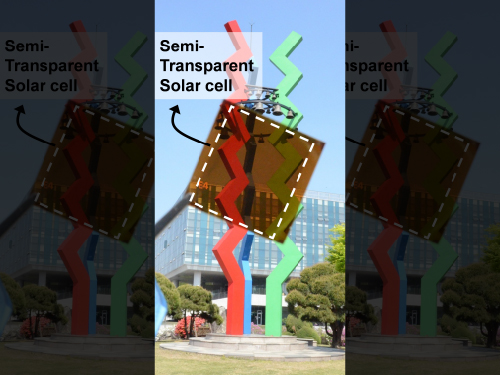
Picture 1: Semi-transparent Perovskite Solar Cell
This picture shows a prototype of a semi-transparent perovskite solar cell with thermal-mirror functionality.
Picture 2: A Heat Rejection Performance Comparison Experiment
This picture presents thermal images taken by an infrared camera for comparing the heat rejection performance of bare glass, automotive tinting film, and a semi-transparent perovskite solar cell after being illuminated by a halogen lamp for five minutes.
2016.08.02 View 10706
KAIST Team Develops Semi-Transparent Solar Cells with Thermal Mirror Capability
A research team led by KAIST and Sungkyunkwan University professors has created semi-transparent perovskite solar cells that demonstrate high-power conversion efficiency and transmit visible light while blocking infrared light, making them great candidates for solar windows.
Modern architects prefer to build exteriors designed with glass mainly from artistic or cost perspectives. Scientists, however, go one step further and see opportunities from its potential ability to harness solar energy. Researchers have thus explored ways to make solar cells transparent or semi-transparent as a substitute material for glass, but this has proven to be a challenging task because solar cells need to absorb sunlight to generate electricity, and when they are transparent, it reduces their energy efficiency.
Typical solar cells today are made of crystalline silicon, but it is difficult to make them translucent. Semi-transparent solar cells under development use, for example, organic or dye-sensitized materials, but compared to crystalline silicon-based cells, their power-conversion efficiencies are relatively low. Perovskites are hybrid organic-inorganic halide-based photovoltaic materials, which are cheap to produce and easy to manufacture. They have recently received much attention as the efficiency of perovskite solar cells has rapidly increased to the level of silicon technologies in the past few years.
Using perovskites, a Korean research team led by Professor Seunghyup Yoo of the Electrical Engineering School at KAIST and Professor Nam-Gyu Park of the Chemical Engineering School at Sungkyunkwan University developed a semi-transparent solar cell that is highly efficient and, additionally, functions very effectively as a thermal-mirror.
The team has developed a top transparent electrode (TTE) that works well with perovskite solar cells. In most cases, a key to success in realizing semi-transparent solar cells is to find a TTE that is compatible with a given photoactive material system, which is also the case for perovskite solar cells. The proposed TTE is based on a multilayer stack consisting of a metal film sandwiched between a high refractive-index (high-index) layer and an interfacial buffer layer. This TTE, placed as a top-most layer, can be prepared without damaging ingredients used in perovskite solar cells. Unlike conventional transparent electrodes focusing only on transmitting visible light, the proposed TTE plays the dual role of passing through visible light while reflecting infrared rays. The semi-transparent solar cells made with the proposed TTEs exhibited average power conversion efficiency as high as 13.3% with 85.5% infrared rejection.
The team believes that if the semi-transparent perovskite solar cells are scaled up for practical applications, they can be used in solar windows for buildings and automobiles, which not only generate electrical energy but also enable the smart heat management for indoor environments, thereby utilizing solar energy more efficiently and effectively.
This result was published as a cover article in the July 20, 2016 issue of Advanced Energy Materials. The research paper is entitled “Empowering Semi-transparent Solar Cells with Thermal-mirror Functionality.” (DOI: 10.1002/aenm.201502466)
The team designed the transparent electrode (TE) stack in three layers: A thin-film of silver (Ag) is placed in between the bottom interfacial layer of molybdenum trioxide (MoO3) and the top high-index dielectric layer of zinc sulfide (ZnS). Such a tri-layer approach has been known as a means to increase the overall visible-light transmittance of metallic thin films via index matching technique, which is essentially the same technique used for anti-reflection coating of glasses except that the present case involves a metallic layer.
Traditionally, when a TE is based on a metal film, such as Ag, the film should be extremely thin, e.g., 7-12 nanometers (nm), to obtain transparency and, accordingly, to transmit visible light. However, the team took a different approach in this research. They made the Ag TE two or three times thicker (12-24 nm) than conventional metal films and, as a result, it reflected more infrared light. The high refractive index of the ZnS layer plays an essential role in keeping the visible light transmittance of the proposed TTE high even with the relatively thick Ag film when its thickness is carefully optimized for maximal destructive interference, leading to low reflectance (and thus high transmittance) within its visible light range.
The team confirmed the semi-transparent perovskite solar cell’s thermal-mirror function through an experiment in which a halogen lamp illuminated an object for five minutes through three mediums: a window of bare glass, automotive tinting film, and the proposed semi-transparent perovskite solar cell. An infrared (IR) camera took thermal images of the object as well as that of each window’s surface. The object’s temperature, when exposed through the glass window, rose to 36.8 Celsius degrees whereas both the tinting film and the cell allowed the object to remain below 27 Celsius degrees. The tinting film absorbs light to block solar energy, so the film’s surface became hot as it was continuously exposed to the lamp light, but the proposed semi-transparent solar cell stayed cool since it rejects solar heat energy by reflection, rather than by absorption. The total solar energy rejection (TSER) of the proposed cell was as high as 89.6%.
Professor Yoo of KAIST said, “The major contributions of this work are to find transparent electrode technology suitable for translucent perovskite cells and to provide a design approach to fully harness the potential it can further deliver as a heat mirror in addition to its main role as an electrode. The present work can be further fine-tuned to include colored solar cells and to incorporate flexible or rollable form factors, as they will allow for greater design freedom and thus offer more opportunities for them to be integrated into real-world objects and structures such as cars, buildings, and houses.”
The lead authors are Hoyeon Kim and Jaewon Ha, both Ph.D. candidates in the School of Electrical Engineering at KAIST, and Hui-Seon Kim, a student in the School of Chemical Engineering at Sungkyunkwan University. This research was supported mainly by the Climate Change Research Hub Program of KAIST.
Picture 1: Semi-transparent Perovskite Solar Cell
This picture shows a prototype of a semi-transparent perovskite solar cell with thermal-mirror functionality.
Picture 2: A Heat Rejection Performance Comparison Experiment
This picture presents thermal images taken by an infrared camera for comparing the heat rejection performance of bare glass, automotive tinting film, and a semi-transparent perovskite solar cell after being illuminated by a halogen lamp for five minutes.
2016.08.02 View 10706 -
 Graphene-Based Transparent Electrodes for Highly Efficient Flexible OLEDs
A Korean research team developed an ideal electrode structure composed of graphene and layers of titanium dioxide and conducting polymers, resulting in highly flexible and efficient OLEDs.
The arrival of a thin and lightweight computer that even rolls up like a piece of paper will not be in the far distant future. Flexible organic light-emitting diodes (OLEDs), built upon a plastic substrate, have received greater attention lately for their use in next-generation displays that can be bent or rolled while still operating.
A Korean research team led by Professor Seunghyup Yoo from the School of Electrical Engineering, KAIST and Professor Tae-Woo Lee from the Department of Materials Science and Engineering, Pohang University of Science and Technology (POSTECH) has developed highly flexible OLEDs with excellent efficiency by using graphene as a transparent electrode (TE) which is placed in between titanium dioxide (TiO2) and conducting polymer layers. The research results were published online on June 2, 2016 in Nature Communications.
OLEDs are stacked in several ultra-thin layers on glass, foil, or plastic substrates, in which multi-layers of organic compounds are sandwiched between two electrodes (cathode and anode). When voltage is applied across the electrodes, electrons from the cathode and holes (positive charges) from the anode draw toward each other and meet in the emissive layer. OLEDs emit light as an electron recombines with a positive hole, releasing energy in the form of a photon. One of the electrodes in OLEDs is usually transparent, and depending on which electrode is transparent, OLEDs can either emit from the top or bottom.
In conventional bottom-emission OLEDs, an anode is transparent in order for the emitted photons to exit the device through its substrate. Indium-tin-oxide (ITO) is commonly used as a transparent anode because of its high transparency, low sheet resistance, and well-established manufacturing process. However, ITO can potentially be expensive, and moreover, is brittle, being susceptible to bending-induced formation of cracks.
Graphene, a two-dimensional thin layer of carbon atoms tightly bonded together in a hexagonal honeycomb lattice, has recently emerged as an alternative to ITO. With outstanding electrical, physical, and chemical properties, its atomic thinness leading to a high degree of flexibility and transparency makes it an ideal candidate for TEs. Nonetheless, the efficiency of graphene-based OLEDs reported to date has been, at best, about the same level of ITO-based OLEDs.
As a solution, the Korean research team, which further includes Professors Sung-Yool Choi (Electrical Engineering) and Taek-Soo Kim (Mechanical Engineering) of KAIST and their students, proposed a new device architecture that can maximize the efficiency of graphene-based OLEDs. They fabricated a transparent anode in a composite structure in which a TiO2 layer with a high refractive index (high-n) and a hole-injection layer (HIL) of conducting polymers with a low refractive index (low-n) sandwich graphene electrodes. This is an optical design that induces a synergistic collaboration between the high-n and low-n layers to increase the effective reflectance of TEs. As a result, the enhancement of the optical cavity resonance is maximized. The optical cavity resonance is related to the improvement of efficiency and color gamut in OLEDs. At the same time, the loss from surface plasmon polariton (SPP), a major cause for weak photon emissions in OLEDs, is also reduced due to the presence of the low-n conducting polymers.
Under this approach, graphene-based OLEDs exhibit 40.8% of ultrahigh external quantum efficiency (EQE) and 160.3 lm/W of power efficiency, which is unprecedented in those using graphene as a TE. Furthermore, these devices remain intact and operate well even after 1,000 bending cycles at a radius of curvature as small as 2.3 mm. This is a remarkable result for OLEDs containing oxide layers such as TiO2 because oxides are typically brittle and prone to bending-induced fractures even at a relatively low strain. The research team discovered that TiO2 has a crack-deflection toughening mechanism that tends to prevent bending-induced cracks from being formed easily.
Professor Yoo said, “What’s unique and advanced about this technology, compared with previous graphene-based OLEDs, is the synergistic collaboration of high- and low-index layers that enables optical management of both resonance effect and SPP loss, leading to significant enhancement in efficiency, all with little compromise in flexibility.” He added, “Our work was the achievement of collaborative research, transcending the boundaries of different fields, through which we have often found meaningful breakthroughs.”
Professor Lee said, “We expect that our technology will pave the way to develop an OLED light source for highly flexible and wearable displays, or flexible sensors that can be attached to the human body for health monitoring, for instance.”
The research paper is entitled “Synergistic Electrode Architecture for Efficient Graphene-based Flexible Organic Light-emitting Diodes” (DOI. 10.1038/NCOMMS11791). The lead authors are Jae-Ho Lee, a Ph.D. candidate at KAIST; Tae-Hee Han, a Ph.D. researcher at POSTECH; and Min-Ho Park, a Ph.D. candidate at POSTECH.
This study was supported by the Basic Science Research Program of the National Research Foundation of Korea (NRF) through the Center for Advanced Flexible Display (CAFDC) funded by the Ministry of Science, ICT and Future Planning (MSIP); by the Center for Advanced Soft-Electronics funded by the MSIP as a Global Frontier Project; by the Graphene Research Center Program of KAIST; and by grants from the IT R&D Program of the Ministry of Trade, Industry and Energy of Korea (MOTIE).
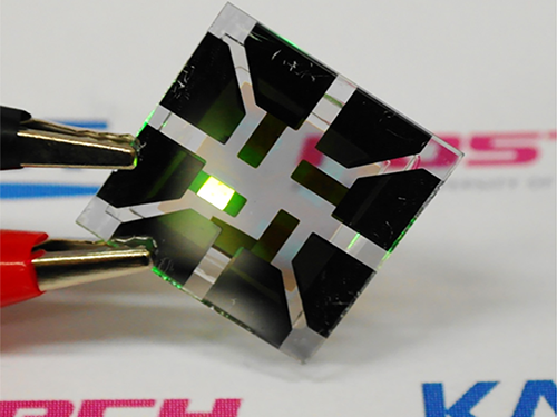
Figure 1: Application of Graphene-based OLEDs
This picture shows an OLED with the composite structure of TiO2/graphene/conducting polymer electrode in operation. The OLED exhibits 40.8% of ultrahigh external quantum efficiency (EQE) and 160.3 lm/W of power efficiency. The device prepared on a plastic substrate shown in the right remains intact and operates well even after 1,000 bending cycles at a radius of curvature as small as 2.3 mm.
Figure 2: Schematic Device Structure of Graphene-based OLEDs
This picture shows the new architecture to develop highly flexible OLEDs with excellent efficiency by using graphene as a transparent electrode (TE).
2016.06.07 View 11295
Graphene-Based Transparent Electrodes for Highly Efficient Flexible OLEDs
A Korean research team developed an ideal electrode structure composed of graphene and layers of titanium dioxide and conducting polymers, resulting in highly flexible and efficient OLEDs.
The arrival of a thin and lightweight computer that even rolls up like a piece of paper will not be in the far distant future. Flexible organic light-emitting diodes (OLEDs), built upon a plastic substrate, have received greater attention lately for their use in next-generation displays that can be bent or rolled while still operating.
A Korean research team led by Professor Seunghyup Yoo from the School of Electrical Engineering, KAIST and Professor Tae-Woo Lee from the Department of Materials Science and Engineering, Pohang University of Science and Technology (POSTECH) has developed highly flexible OLEDs with excellent efficiency by using graphene as a transparent electrode (TE) which is placed in between titanium dioxide (TiO2) and conducting polymer layers. The research results were published online on June 2, 2016 in Nature Communications.
OLEDs are stacked in several ultra-thin layers on glass, foil, or plastic substrates, in which multi-layers of organic compounds are sandwiched between two electrodes (cathode and anode). When voltage is applied across the electrodes, electrons from the cathode and holes (positive charges) from the anode draw toward each other and meet in the emissive layer. OLEDs emit light as an electron recombines with a positive hole, releasing energy in the form of a photon. One of the electrodes in OLEDs is usually transparent, and depending on which electrode is transparent, OLEDs can either emit from the top or bottom.
In conventional bottom-emission OLEDs, an anode is transparent in order for the emitted photons to exit the device through its substrate. Indium-tin-oxide (ITO) is commonly used as a transparent anode because of its high transparency, low sheet resistance, and well-established manufacturing process. However, ITO can potentially be expensive, and moreover, is brittle, being susceptible to bending-induced formation of cracks.
Graphene, a two-dimensional thin layer of carbon atoms tightly bonded together in a hexagonal honeycomb lattice, has recently emerged as an alternative to ITO. With outstanding electrical, physical, and chemical properties, its atomic thinness leading to a high degree of flexibility and transparency makes it an ideal candidate for TEs. Nonetheless, the efficiency of graphene-based OLEDs reported to date has been, at best, about the same level of ITO-based OLEDs.
As a solution, the Korean research team, which further includes Professors Sung-Yool Choi (Electrical Engineering) and Taek-Soo Kim (Mechanical Engineering) of KAIST and their students, proposed a new device architecture that can maximize the efficiency of graphene-based OLEDs. They fabricated a transparent anode in a composite structure in which a TiO2 layer with a high refractive index (high-n) and a hole-injection layer (HIL) of conducting polymers with a low refractive index (low-n) sandwich graphene electrodes. This is an optical design that induces a synergistic collaboration between the high-n and low-n layers to increase the effective reflectance of TEs. As a result, the enhancement of the optical cavity resonance is maximized. The optical cavity resonance is related to the improvement of efficiency and color gamut in OLEDs. At the same time, the loss from surface plasmon polariton (SPP), a major cause for weak photon emissions in OLEDs, is also reduced due to the presence of the low-n conducting polymers.
Under this approach, graphene-based OLEDs exhibit 40.8% of ultrahigh external quantum efficiency (EQE) and 160.3 lm/W of power efficiency, which is unprecedented in those using graphene as a TE. Furthermore, these devices remain intact and operate well even after 1,000 bending cycles at a radius of curvature as small as 2.3 mm. This is a remarkable result for OLEDs containing oxide layers such as TiO2 because oxides are typically brittle and prone to bending-induced fractures even at a relatively low strain. The research team discovered that TiO2 has a crack-deflection toughening mechanism that tends to prevent bending-induced cracks from being formed easily.
Professor Yoo said, “What’s unique and advanced about this technology, compared with previous graphene-based OLEDs, is the synergistic collaboration of high- and low-index layers that enables optical management of both resonance effect and SPP loss, leading to significant enhancement in efficiency, all with little compromise in flexibility.” He added, “Our work was the achievement of collaborative research, transcending the boundaries of different fields, through which we have often found meaningful breakthroughs.”
Professor Lee said, “We expect that our technology will pave the way to develop an OLED light source for highly flexible and wearable displays, or flexible sensors that can be attached to the human body for health monitoring, for instance.”
The research paper is entitled “Synergistic Electrode Architecture for Efficient Graphene-based Flexible Organic Light-emitting Diodes” (DOI. 10.1038/NCOMMS11791). The lead authors are Jae-Ho Lee, a Ph.D. candidate at KAIST; Tae-Hee Han, a Ph.D. researcher at POSTECH; and Min-Ho Park, a Ph.D. candidate at POSTECH.
This study was supported by the Basic Science Research Program of the National Research Foundation of Korea (NRF) through the Center for Advanced Flexible Display (CAFDC) funded by the Ministry of Science, ICT and Future Planning (MSIP); by the Center for Advanced Soft-Electronics funded by the MSIP as a Global Frontier Project; by the Graphene Research Center Program of KAIST; and by grants from the IT R&D Program of the Ministry of Trade, Industry and Energy of Korea (MOTIE).
Figure 1: Application of Graphene-based OLEDs
This picture shows an OLED with the composite structure of TiO2/graphene/conducting polymer electrode in operation. The OLED exhibits 40.8% of ultrahigh external quantum efficiency (EQE) and 160.3 lm/W of power efficiency. The device prepared on a plastic substrate shown in the right remains intact and operates well even after 1,000 bending cycles at a radius of curvature as small as 2.3 mm.
Figure 2: Schematic Device Structure of Graphene-based OLEDs
This picture shows the new architecture to develop highly flexible OLEDs with excellent efficiency by using graphene as a transparent electrode (TE).
2016.06.07 View 11295 -
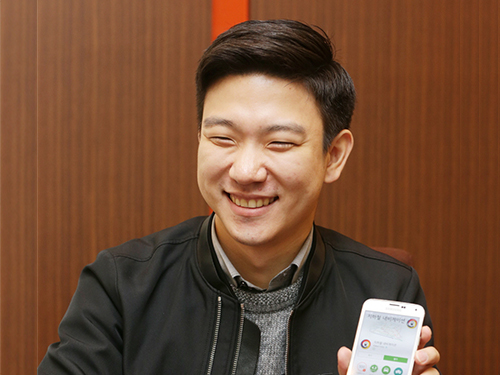 A KAIST Student Donates USD 26,000 to His Alma Mater
A KAIST undergraduate student who developed and sold a smart phone application donated USD 26,000 to his alma mater.
Seung-Kyu Oh of the School of Electrical Engineering gave his donation to President Steve Kang of KAIST on November 24, 2015. This is the largest amount donated by an enrolled undergraduate.
In 2010, at a time when android smart phones were just being released, Mr. Oh decided to develop a subway app because existing subway apps were not user-friendly.
Mr. Oh’s “Subway Navigation” app checks the current operation hours and gives users the shortest path when the user selects points of departure and arrival. The calculation for the shortest path involves factors such as which train comes first, where and to what train to transfer, the first and last trains of the day, transfer passageway usage time, etc.
To make the app useful to the largest number of people, Mr. Oh distributed it on the open market. Currently, the app is ranked the second most downloaded subway app, and has even made considerable advertising profits, having accumulated more than 5,000,000 users. This year, Mr. Oh received an offer from Kakao, an Internet company based in Seoul, Korea, to take over the app and sold it to them.
Mr. Oh said that making a donation KAIST was the first thing that came to his mind when he earned this profit.
Mr. Oh, who graduated from the Korea Science Academy, a science magnet high school, said that he felt a sense of responsibility for receiving support from Korea since high school, and that he decided to donate to KAIST as a way of returning the support that he had received so far.
He further said that “if an individual’s efforts and talents created some profit together with what he or she learned from school, then the school that supported the student in furthering his studies has also played a significant role,” and that “likewise, our stellar alumni can contribute more to our younger classmates’ growth and development.”
Mr. Oh, who is at his last semester, plans to join Kakao and will take on a job managing his subway app.
President Kang said he hopes that “all KAISTians will emulate Mr. Oh’s example to support the school” and that “the university will use the money to invest further in its future.”
2015.11.24 View 3828
A KAIST Student Donates USD 26,000 to His Alma Mater
A KAIST undergraduate student who developed and sold a smart phone application donated USD 26,000 to his alma mater.
Seung-Kyu Oh of the School of Electrical Engineering gave his donation to President Steve Kang of KAIST on November 24, 2015. This is the largest amount donated by an enrolled undergraduate.
In 2010, at a time when android smart phones were just being released, Mr. Oh decided to develop a subway app because existing subway apps were not user-friendly.
Mr. Oh’s “Subway Navigation” app checks the current operation hours and gives users the shortest path when the user selects points of departure and arrival. The calculation for the shortest path involves factors such as which train comes first, where and to what train to transfer, the first and last trains of the day, transfer passageway usage time, etc.
To make the app useful to the largest number of people, Mr. Oh distributed it on the open market. Currently, the app is ranked the second most downloaded subway app, and has even made considerable advertising profits, having accumulated more than 5,000,000 users. This year, Mr. Oh received an offer from Kakao, an Internet company based in Seoul, Korea, to take over the app and sold it to them.
Mr. Oh said that making a donation KAIST was the first thing that came to his mind when he earned this profit.
Mr. Oh, who graduated from the Korea Science Academy, a science magnet high school, said that he felt a sense of responsibility for receiving support from Korea since high school, and that he decided to donate to KAIST as a way of returning the support that he had received so far.
He further said that “if an individual’s efforts and talents created some profit together with what he or she learned from school, then the school that supported the student in furthering his studies has also played a significant role,” and that “likewise, our stellar alumni can contribute more to our younger classmates’ growth and development.”
Mr. Oh, who is at his last semester, plans to join Kakao and will take on a job managing his subway app.
President Kang said he hopes that “all KAISTians will emulate Mr. Oh’s example to support the school” and that “the university will use the money to invest further in its future.”
2015.11.24 View 3828 -
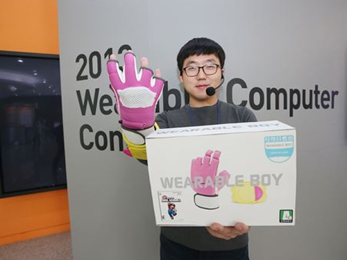
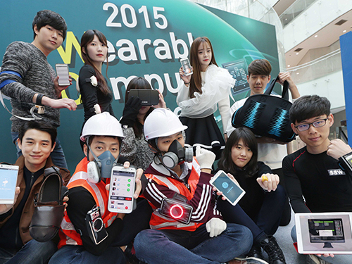 KAIST Hosts the Wearable Computer Contest 2015
“What you see is a compact electronic system on a dust mask, which monitors the amount of dust taken in by a worker and lets other workers know if the person is injured in an industrial site,” said Bum Taek Jung, a Master’s candidate from Sungkyunkwan University during the Wearable Computer Contest 2015 held in KI building of KAIST on November 5, 2015.
He explained his interest in developing this system, “Dust-related respiratory diseases and falling accidents are still prevalent in industrial sites.” He added, “Using the smart dust mask helps monitoring workers’ physical condition in real time, allowing us to cope with accidents in a much more timely manner.” A smart dust mask is a portable device that alerts the user with orange or red light signs when the amount of dust inhaled by the user is higher than the threshold. Its application on a smartphone can also allow project managers to alert the risk of falling accidents to workers by employing a gyroscope and an accelerometer on the mask.
The Wearable Computer Contest 2015 met for the eleventh time at KAIST on November 5-6, 2015. A wearable computer refers to a portable device which users can wear directly on the body or on their clothes while moving. Products that can provide various services by connecting to a smartphone have become increasingly popular. The contest is an excellent opportunity for university students to design creative wearable systems similar to those often depicted in movies and comics.
This year 102 teams from universities all over the nation participated. After screening and evaluation of their presentations, only 8 teams in the product section and 3 teams in the ideas section were selected for the finals. Of the many entries to the contest, the ECG security system caught many people’s attention. The wearable, which attaches to a shirt, acts like an electrocardiogram. By comparing the ECG reading with the one stored in the data server, the wearable can authenticate the user. The system could be widely used by enterprises and financial companies where tight security and authentication are crucial.
The winners of the product and the ideas sections received USD 4,300 and usd 860 respectively along with Minister Prizes from the Minister of Science, ICT and Future Planning of Korea. The Chairman of the contest, Professor Hoi-Jun Yoo from the Electrical Engineering Department of KAIST said, “The contest will be a great opportunity for anyone to have a look at advanced wearable devices developed through close integration of state-of-the-art technologies and creative ideas from young minds.”
2015.11.05 View 6238
KAIST Hosts the Wearable Computer Contest 2015
“What you see is a compact electronic system on a dust mask, which monitors the amount of dust taken in by a worker and lets other workers know if the person is injured in an industrial site,” said Bum Taek Jung, a Master’s candidate from Sungkyunkwan University during the Wearable Computer Contest 2015 held in KI building of KAIST on November 5, 2015.
He explained his interest in developing this system, “Dust-related respiratory diseases and falling accidents are still prevalent in industrial sites.” He added, “Using the smart dust mask helps monitoring workers’ physical condition in real time, allowing us to cope with accidents in a much more timely manner.” A smart dust mask is a portable device that alerts the user with orange or red light signs when the amount of dust inhaled by the user is higher than the threshold. Its application on a smartphone can also allow project managers to alert the risk of falling accidents to workers by employing a gyroscope and an accelerometer on the mask.
The Wearable Computer Contest 2015 met for the eleventh time at KAIST on November 5-6, 2015. A wearable computer refers to a portable device which users can wear directly on the body or on their clothes while moving. Products that can provide various services by connecting to a smartphone have become increasingly popular. The contest is an excellent opportunity for university students to design creative wearable systems similar to those often depicted in movies and comics.
This year 102 teams from universities all over the nation participated. After screening and evaluation of their presentations, only 8 teams in the product section and 3 teams in the ideas section were selected for the finals. Of the many entries to the contest, the ECG security system caught many people’s attention. The wearable, which attaches to a shirt, acts like an electrocardiogram. By comparing the ECG reading with the one stored in the data server, the wearable can authenticate the user. The system could be widely used by enterprises and financial companies where tight security and authentication are crucial.
The winners of the product and the ideas sections received USD 4,300 and usd 860 respectively along with Minister Prizes from the Minister of Science, ICT and Future Planning of Korea. The Chairman of the contest, Professor Hoi-Jun Yoo from the Electrical Engineering Department of KAIST said, “The contest will be a great opportunity for anyone to have a look at advanced wearable devices developed through close integration of state-of-the-art technologies and creative ideas from young minds.”
2015.11.05 View 6238 -
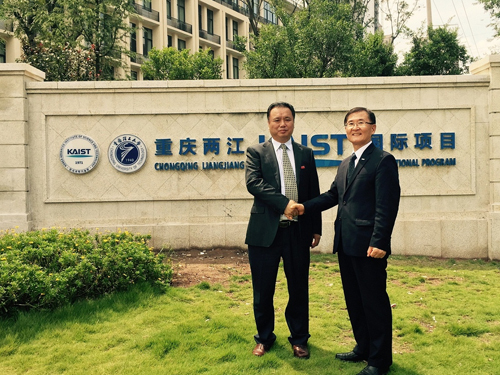 KAIST and Chongqing University of Technology in China Open an International Program
With the help of KAIST, Chongqing University of Technology (CQUT) in China established an electrical engineering and computer science program and admitted their first 66 freshmen this fall semester.
The joint program was created to foster skilled engineers in the fields of electrical engineering and computer science, which are necessary for the development of the Korean and Chinese Industrial Complex located in Chongqing City.
KAIST has provided CQUT with a majority of the program’s curricula currently offered to its students in Daejeon, Korea.
Under the jointly administered program, KAIST takes on education and research while CQUT is responsible for student selection and administration.
KAIST has dispatched eight professors to teach the related fields in English, and 17 CQUT professors will teach the rest of the curricula.
In August 2014, KAIST and CQUT singed a cooperation agreement for education and research exchange and created the CQUT-KAIST Education Cooperation Center, which is headed by Professor Young-Nam Han of the Electrical Engineering Department at KAIST.
The two universities will expand their collaboration to include graduate programs by 2016.
In the picture below, President Steve Kang of KAIST (right) shakes hands with President Shi Xiaohui of Chongqing University of Technology (left).
2015.09.17 View 7891
KAIST and Chongqing University of Technology in China Open an International Program
With the help of KAIST, Chongqing University of Technology (CQUT) in China established an electrical engineering and computer science program and admitted their first 66 freshmen this fall semester.
The joint program was created to foster skilled engineers in the fields of electrical engineering and computer science, which are necessary for the development of the Korean and Chinese Industrial Complex located in Chongqing City.
KAIST has provided CQUT with a majority of the program’s curricula currently offered to its students in Daejeon, Korea.
Under the jointly administered program, KAIST takes on education and research while CQUT is responsible for student selection and administration.
KAIST has dispatched eight professors to teach the related fields in English, and 17 CQUT professors will teach the rest of the curricula.
In August 2014, KAIST and CQUT singed a cooperation agreement for education and research exchange and created the CQUT-KAIST Education Cooperation Center, which is headed by Professor Young-Nam Han of the Electrical Engineering Department at KAIST.
The two universities will expand their collaboration to include graduate programs by 2016.
In the picture below, President Steve Kang of KAIST (right) shakes hands with President Shi Xiaohui of Chongqing University of Technology (left).
2015.09.17 View 7891 -
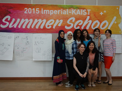 KAIST Operates a Summer School with Imperial College London
KAIST and Imperial College London jointly hosted a summer school on the KAIST campus on July 14-17, 2015. Twenty-five students from both universities, 11 from KAIST and 14 from Imperial College, participated in the summer program.
KAIST and Imperial College agreed to hold academic and research exchange programs in 2013; this year’s summer school represented the first effort.
Participants were divided into a few cohorts of four or five students. They conducted a series of activities to implement joint research projects involving team building, networking, joint study, discussions, and presentations.
Among the projects the summer school ran, Professor Hoi-Jun Yoo of the Electrical Engineering Department at KAIST was invited to teach students about the mobile healthcare system, Dr. M, that he had developed.
Sung-Hyon Myaeng, Associate Vice President of the International Affairs Office, KAIST, said, “This summer school is yet another example of KAIST’s ongoing efforts to make the campus more global and to interact actively with members of the international community.”
2015.07.29 View 6574
KAIST Operates a Summer School with Imperial College London
KAIST and Imperial College London jointly hosted a summer school on the KAIST campus on July 14-17, 2015. Twenty-five students from both universities, 11 from KAIST and 14 from Imperial College, participated in the summer program.
KAIST and Imperial College agreed to hold academic and research exchange programs in 2013; this year’s summer school represented the first effort.
Participants were divided into a few cohorts of four or five students. They conducted a series of activities to implement joint research projects involving team building, networking, joint study, discussions, and presentations.
Among the projects the summer school ran, Professor Hoi-Jun Yoo of the Electrical Engineering Department at KAIST was invited to teach students about the mobile healthcare system, Dr. M, that he had developed.
Sung-Hyon Myaeng, Associate Vice President of the International Affairs Office, KAIST, said, “This summer school is yet another example of KAIST’s ongoing efforts to make the campus more global and to interact actively with members of the international community.”
2015.07.29 View 6574 -
 World Renowned Wireless Technology Experts Gathered in KAIST
KAIST hosted the 2015 IEEE WoW from June 5 to 6, 2015
Wireless power transfer technologies, such as wireless electric vehicles, trains and batteries, are increasingly in use. A conference, The 2015 IEEE WoW (Workshop on Wireless Power), was held in KI Building for two days starting June 5, 2015 to exchange ideas on the new trends and issues of the world wireless power technology.
The wireless power conference hosted by Institute of Electrical and Electronics Engineers (IEEE), IEEE WoW, was sponsored by its societies, PELS, IAS, IES, VTS, MAG, and PES.
This year’s conference took place in Korea for the first time and was titled “IEEE PELS Workshop on Emerging Technologies: Wireless Power.” The event was attended by around 200 experts in wireless power from 15 countries to discuss the international standards and current trends.
Keynote speakers were President Don Tan of IEEE; Professor Grant Covic of the University of Auckland; Andrew Daga, the CEO at Momentum Dynamics Corporation; Professor Ron Hui of the City University of Hong Kong; and Jung Goo Cho, the CEO of Green Power Technologies.
The forum included plenary speaking sessions on “The Futures of EV and Power Electronics,” “Development of IPT at the University of Auckland,” “Interoperable Solution for Wireless EV Charging,” “Development of IPT for Factory Automation,” “Commercialization of High Power WPT,” and “WPT: From Directional Power to Omni-directional Power.”
Notably, KAIST Professor Dong-Ho Cho, responsible for KAIST’s On-Line Electric Vehicle (OLEV) development, spoke on “The Development of Shaped Magnetic Field Systems for EVs and Trains” to introduce the KAIST OLEV bus and OLEV trains developed in cooperation with Korea Railroad Research Institute.
The Dialog Sessions on “The Futures of Wireless Electric Vehicles” were led by John M. Miller of JNJ Miller and “Road Charged EV and WPT Regulation and Standard for EV in Japan” by Yoichi Hori of University of Tokyo.
The General Chair of this year’s IEEE WoW, KAIST Professor Chun T. Rim said, “This forum serves a great assistance to the industry using wireless power technology in areas such as smartphones, home appliances, Internet of Things, and wearable devices.”
2015.05.29 View 7224
World Renowned Wireless Technology Experts Gathered in KAIST
KAIST hosted the 2015 IEEE WoW from June 5 to 6, 2015
Wireless power transfer technologies, such as wireless electric vehicles, trains and batteries, are increasingly in use. A conference, The 2015 IEEE WoW (Workshop on Wireless Power), was held in KI Building for two days starting June 5, 2015 to exchange ideas on the new trends and issues of the world wireless power technology.
The wireless power conference hosted by Institute of Electrical and Electronics Engineers (IEEE), IEEE WoW, was sponsored by its societies, PELS, IAS, IES, VTS, MAG, and PES.
This year’s conference took place in Korea for the first time and was titled “IEEE PELS Workshop on Emerging Technologies: Wireless Power.” The event was attended by around 200 experts in wireless power from 15 countries to discuss the international standards and current trends.
Keynote speakers were President Don Tan of IEEE; Professor Grant Covic of the University of Auckland; Andrew Daga, the CEO at Momentum Dynamics Corporation; Professor Ron Hui of the City University of Hong Kong; and Jung Goo Cho, the CEO of Green Power Technologies.
The forum included plenary speaking sessions on “The Futures of EV and Power Electronics,” “Development of IPT at the University of Auckland,” “Interoperable Solution for Wireless EV Charging,” “Development of IPT for Factory Automation,” “Commercialization of High Power WPT,” and “WPT: From Directional Power to Omni-directional Power.”
Notably, KAIST Professor Dong-Ho Cho, responsible for KAIST’s On-Line Electric Vehicle (OLEV) development, spoke on “The Development of Shaped Magnetic Field Systems for EVs and Trains” to introduce the KAIST OLEV bus and OLEV trains developed in cooperation with Korea Railroad Research Institute.
The Dialog Sessions on “The Futures of Wireless Electric Vehicles” were led by John M. Miller of JNJ Miller and “Road Charged EV and WPT Regulation and Standard for EV in Japan” by Yoichi Hori of University of Tokyo.
The General Chair of this year’s IEEE WoW, KAIST Professor Chun T. Rim said, “This forum serves a great assistance to the industry using wireless power technology in areas such as smartphones, home appliances, Internet of Things, and wearable devices.”
2015.05.29 View 7224 -
 Workshop on Wearable Healthcare Takes Place on July 15, 2014
A workshop on wearable healthcare was held at KAIST campus on July 15, 2014.
In recent years, wearable healthcare has received much attention as an emerging technology that will have a great impact on our society.
At the workshop, participants from academia and industry reviewed the Korean healthcare industry and discussed issues related to the development of a wearable healthcare industry in Korea, while capitalizing on the nation’s strength in information and communications.
Professor Hoi-Jun Yoo of Electrical Engineering at KAIST, the chairman of the organizing committee of the workshop, presented a keynote speech entitled “The Current State and Future of Wearable Healthcare,” arguing that the wearable healthcare industry developed through the Internet of things and big data would become the next-generation growth engine for Korea.
Other key presentations were “Smart Glasses and Micro Display Semiconductor Technology” by Bo-Eun Kim, Chief Executive Officer of Raon-Tech, Inc., “Wearable Device: A Comprehensive Approach” by Min-Kyu Je, a professor of Daegu Gyeongbuk Institute of Science and Technology, and “Microwave Imaging System for Breast Cancer Detection” by Seung-Joon Lee, a professor of Ewha Woman’s University.
Professor Yoo said, “We hope that the workshop will provide good momentum for participants to evaluate the Korean healthcare industry in the context of the Internet of things, information and communications technology, and medical technology as well as offering practical solutions to nurture the indigenous wearable healthcare industry in Korea.”
2014.07.15 View 7625
Workshop on Wearable Healthcare Takes Place on July 15, 2014
A workshop on wearable healthcare was held at KAIST campus on July 15, 2014.
In recent years, wearable healthcare has received much attention as an emerging technology that will have a great impact on our society.
At the workshop, participants from academia and industry reviewed the Korean healthcare industry and discussed issues related to the development of a wearable healthcare industry in Korea, while capitalizing on the nation’s strength in information and communications.
Professor Hoi-Jun Yoo of Electrical Engineering at KAIST, the chairman of the organizing committee of the workshop, presented a keynote speech entitled “The Current State and Future of Wearable Healthcare,” arguing that the wearable healthcare industry developed through the Internet of things and big data would become the next-generation growth engine for Korea.
Other key presentations were “Smart Glasses and Micro Display Semiconductor Technology” by Bo-Eun Kim, Chief Executive Officer of Raon-Tech, Inc., “Wearable Device: A Comprehensive Approach” by Min-Kyu Je, a professor of Daegu Gyeongbuk Institute of Science and Technology, and “Microwave Imaging System for Breast Cancer Detection” by Seung-Joon Lee, a professor of Ewha Woman’s University.
Professor Yoo said, “We hope that the workshop will provide good momentum for participants to evaluate the Korean healthcare industry in the context of the Internet of things, information and communications technology, and medical technology as well as offering practical solutions to nurture the indigenous wearable healthcare industry in Korea.”
2014.07.15 View 7625 -
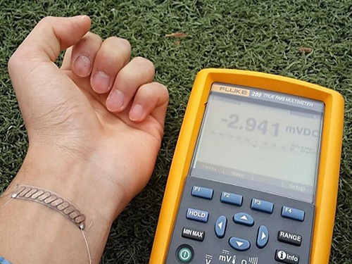 Thermoelectric generator on glass fabric for wearable electronic devices
Wearable computers or devices have been hailed as the next generation of mobile electronic gadgets, from smart watches to smart glasses to smart pacemakers. For electronics to be worn by a user, they must be light, flexible, and equipped with a power source, which could be a portable, long-lasting battery or no battery at all but a generator. How to supply power in a stable and reliable manner is one of the most critical issues to commercialize wearable devices.
A team of KAIST researchers headed by Byung Jin Cho, a professor of electrical engineering, proposed a solution to this problem by developing a glass fabric-based thermoelectric (TE) generator that is extremely light and flexible and produces electricity from the heat of the human body. In fact, it is so flexible that the allowable bending radius of the generator is as low as 20 mm. There are no changes in performance even if the generator bends upward and downward for up to 120 cycles.
To date, two types of TE generators have been developed based either on organic or inorganic materials. The organic-based TE generators use polymers that are highly flexible and compatible with human skin, ideal for wearable electronics. The polymers, however, have a low power output. Inorganic-based TE generators produce a high electrical energy, but they are heavy, rigid, and bulky.
Professor Cho came up with a new concept and design technique to build a flexible TE generator that minimizes thermal energy loss but maximizes power output. His team synthesized liquid-like pastes of n-type (Bi2Te3) and p-type (Sb2Te3) TE materials and printed them onto a glass fabric by applying a screen printing technique. The pastes permeated through the meshes of the fabric and formed films of TE materials in a range of thickness of several hundreds of microns. As a result, hundreds of TE material dots (in combination of n and p types) were printed and well arranged on a specific area of the glass fabric.
Professor Cho explained that his TE generator has a self-sustaining structure, eliminating thick external substrates (usually made of ceramic or alumina) that hold inorganic TE materials. These substrates have taken away a great portion of thermal energy, a serious setback which causes low output power.
He also commented,
"For our case, the glass fabric itself serves as the upper and lower substrates of a TE generator, keeping the inorganic TE materials in between. This is quite a revolutionary approach to design a generator. In so doing, we were able to significantly reduce the weight of our generator (~0.13g/cm2), which is an essential element for wearable electronics."
When using KAIST's TE generator (with a size of 10 cm x 10 cm) for a wearable wristband device, it will produce around 40 mW electric power based on the temperature difference of 31 °F between human skin and the surrounding air.
Professor Cho further described about the merits of the new generator:
"Our technology presents an easy and simple way of fabricating an extremely flexible, light, and high-performance TE generator. We expect that this technology will find further applications in scale-up systems such as automobiles, factories, aircrafts, and vessels where we see abundant thermal energy being wasted."
This research result was published online in the March 14th issue of Energy & Environmental Science and was entitled "Wearable Thermoelectric Generator Fabricated on Glass Fabric."
Youtube Link: http://www.youtube.com/watch?v=BlN9lvEzCuw&feature=youtu.be
[Picture Captions]
Caption 1: The picture shows a high-performance wearable thermoelectric generator that is extremely flexible and light.
Caption 2: A thermoelectric generator developed as a wristband. The generator can be easily curved along with the shape of human body.
Caption 3: KAIST’s thermoelectric generator can be bent as many as 120 times, but it still shows the same high performance.
2014.04.21 View 18998
Thermoelectric generator on glass fabric for wearable electronic devices
Wearable computers or devices have been hailed as the next generation of mobile electronic gadgets, from smart watches to smart glasses to smart pacemakers. For electronics to be worn by a user, they must be light, flexible, and equipped with a power source, which could be a portable, long-lasting battery or no battery at all but a generator. How to supply power in a stable and reliable manner is one of the most critical issues to commercialize wearable devices.
A team of KAIST researchers headed by Byung Jin Cho, a professor of electrical engineering, proposed a solution to this problem by developing a glass fabric-based thermoelectric (TE) generator that is extremely light and flexible and produces electricity from the heat of the human body. In fact, it is so flexible that the allowable bending radius of the generator is as low as 20 mm. There are no changes in performance even if the generator bends upward and downward for up to 120 cycles.
To date, two types of TE generators have been developed based either on organic or inorganic materials. The organic-based TE generators use polymers that are highly flexible and compatible with human skin, ideal for wearable electronics. The polymers, however, have a low power output. Inorganic-based TE generators produce a high electrical energy, but they are heavy, rigid, and bulky.
Professor Cho came up with a new concept and design technique to build a flexible TE generator that minimizes thermal energy loss but maximizes power output. His team synthesized liquid-like pastes of n-type (Bi2Te3) and p-type (Sb2Te3) TE materials and printed them onto a glass fabric by applying a screen printing technique. The pastes permeated through the meshes of the fabric and formed films of TE materials in a range of thickness of several hundreds of microns. As a result, hundreds of TE material dots (in combination of n and p types) were printed and well arranged on a specific area of the glass fabric.
Professor Cho explained that his TE generator has a self-sustaining structure, eliminating thick external substrates (usually made of ceramic or alumina) that hold inorganic TE materials. These substrates have taken away a great portion of thermal energy, a serious setback which causes low output power.
He also commented,
"For our case, the glass fabric itself serves as the upper and lower substrates of a TE generator, keeping the inorganic TE materials in between. This is quite a revolutionary approach to design a generator. In so doing, we were able to significantly reduce the weight of our generator (~0.13g/cm2), which is an essential element for wearable electronics."
When using KAIST's TE generator (with a size of 10 cm x 10 cm) for a wearable wristband device, it will produce around 40 mW electric power based on the temperature difference of 31 °F between human skin and the surrounding air.
Professor Cho further described about the merits of the new generator:
"Our technology presents an easy and simple way of fabricating an extremely flexible, light, and high-performance TE generator. We expect that this technology will find further applications in scale-up systems such as automobiles, factories, aircrafts, and vessels where we see abundant thermal energy being wasted."
This research result was published online in the March 14th issue of Energy & Environmental Science and was entitled "Wearable Thermoelectric Generator Fabricated on Glass Fabric."
Youtube Link: http://www.youtube.com/watch?v=BlN9lvEzCuw&feature=youtu.be
[Picture Captions]
Caption 1: The picture shows a high-performance wearable thermoelectric generator that is extremely flexible and light.
Caption 2: A thermoelectric generator developed as a wristband. The generator can be easily curved along with the shape of human body.
Caption 3: KAIST’s thermoelectric generator can be bent as many as 120 times, but it still shows the same high performance.
2014.04.21 View 18998 -
 KAIST Holds 'Wearable Computer Contest'
Application for ‘2014 Wearable Computer Contest’ until May 23rd
KAIST is holding the 2014 Wearable Computer Contest (WCC) sponsored by Samsung Electronics in November and is currently receiving applications until May 23rd.
Wearable Computer is a device that can be worn on body or clothing, which allows users to be connected while on the move. It is currently receiving attention as the next generation of computer industry that will replace smart phones.
The Wearable Computer Contest will be held under the topic “Smart Fashion to Simple Life” and will be divided into a designated topic contest and an idea contest.
In the “designated topic contest,” each group will compete with their prototypes based on their own ideas about a wearable computer that combines IT and fashion. A total of 15 teams that enter the finals after a document review will be provided with USD 1,400 for a prototype production, Samsung's smart IT devices, and a systematic training program.
For the “idea contest,” competitors will present their ideas for a wearable computer in a poster format. The teams qualified to continue onto the finals will be given an opportunity to create and exhibit a life-sized model.
Chairman of the Wearable Computer Contest (WCC), Professor Hoejun Yoo from the KAIST Department of Electrical Engineering said, “Wearable Computer is the major future growth industry that will lead IT industry after smart phones. I hope WCC will help nurture the future professionals in the field of wearable computer industry.”
The applications for the Wearable Computer Contest can be found on the main website (http://www.ufcom.org) until May 23rd. Both undergraduate and graduate students can participate as a team for the “designated topic contest,” and there are no qualifications required for those who enter the “idea contest.”
Last year, a total of 104 teams from universities all around Korea has participated in the Wearable Computer Contest. The finalist, team 'Jump' from Chungnam University, received the Award of the Minister of Science, ICT and Future Planning, Republic of Korea.
2014.03.28 View 8536
KAIST Holds 'Wearable Computer Contest'
Application for ‘2014 Wearable Computer Contest’ until May 23rd
KAIST is holding the 2014 Wearable Computer Contest (WCC) sponsored by Samsung Electronics in November and is currently receiving applications until May 23rd.
Wearable Computer is a device that can be worn on body or clothing, which allows users to be connected while on the move. It is currently receiving attention as the next generation of computer industry that will replace smart phones.
The Wearable Computer Contest will be held under the topic “Smart Fashion to Simple Life” and will be divided into a designated topic contest and an idea contest.
In the “designated topic contest,” each group will compete with their prototypes based on their own ideas about a wearable computer that combines IT and fashion. A total of 15 teams that enter the finals after a document review will be provided with USD 1,400 for a prototype production, Samsung's smart IT devices, and a systematic training program.
For the “idea contest,” competitors will present their ideas for a wearable computer in a poster format. The teams qualified to continue onto the finals will be given an opportunity to create and exhibit a life-sized model.
Chairman of the Wearable Computer Contest (WCC), Professor Hoejun Yoo from the KAIST Department of Electrical Engineering said, “Wearable Computer is the major future growth industry that will lead IT industry after smart phones. I hope WCC will help nurture the future professionals in the field of wearable computer industry.”
The applications for the Wearable Computer Contest can be found on the main website (http://www.ufcom.org) until May 23rd. Both undergraduate and graduate students can participate as a team for the “designated topic contest,” and there are no qualifications required for those who enter the “idea contest.”
Last year, a total of 104 teams from universities all around Korea has participated in the Wearable Computer Contest. The finalist, team 'Jump' from Chungnam University, received the Award of the Minister of Science, ICT and Future Planning, Republic of Korea.
2014.03.28 View 8536