research
-
 KAIST Develops AI to Easily Find Promising Materials That Capture Only CO₂
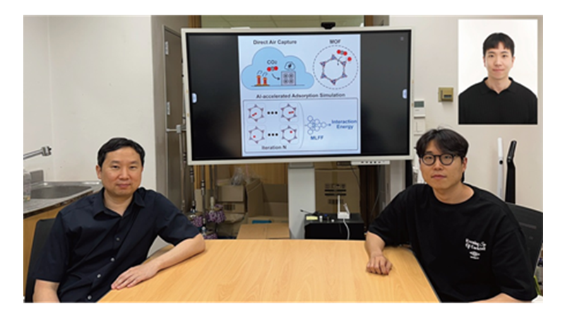
< Photo 1. (From left) Professor Jihan Kim, Ph.D. candidate Yunsung Lim and Dr. Hyunsoo Park of the Department of Chemical and Biomolecular Engineering >
In order to help prevent the climate crisis, actively reducing already-emitted CO₂ is essential. Accordingly, direct air capture (DAC) — a technology that directly extracts only CO₂ from the air — is gaining attention. However, effectively capturing pure CO₂ is not easy due to water vapor (H₂O) present in the air. KAIST researchers have successfully used AI-driven machine learning techniques to identify the most promising CO₂-capturing materials among metal-organic frameworks (MOFs), a key class of materials studied for this technology.
KAIST (President Kwang Hyung Lee) announced on the 29th of June that a research team led by Professor Jihan Kim from the Department of Chemical and Biomolecular Engineering, in collaboration with a team at Imperial College London, has developed a machine-learning-based simulation method that can quickly and accurately screen MOFs best suited for atmospheric CO₂ capture.
< Figure 1. Concept diagram of Direct Air Capture (DAC) technology and carbon capture using Metal-Organic Frameworks (MOFs). MOFs are promising porous materials capable of capturing carbon dioxide from the atmosphere, drawing attention as a core material for DAC technology. >
To overcome the difficulty of discovering high-performance materials due to the complexity of structures and the limitations of predicting intermolecular interactions, the research team developed a machine learning force field (MLFF) capable of precisely predicting the interactions between CO₂, water (H₂O), and MOFs. This new method enables calculations of MOF adsorption properties with quantum-mechanics-level accuracy at vastly faster speeds than before.
Using this system, the team screened over 8,000 experimentally synthesized MOF structures, identifying more than 100 promising candidates for CO₂ capture. Notably, this included new candidates that had not been uncovered by traditional force-field-based simulations. The team also analyzed the relationships between MOF chemical structure and adsorption performance, proposing seven key chemical features that will help in designing new materials for DAC.
< Figure 2. Concept diagram of adsorption simulation using Machine Learning Force Field (MLFF). The developed MLFF is applicable to various MOF structures and allows for precise calculation of adsorption properties by predicting interaction energies during repetitive Widom insertion simulations. It is characterized by simultaneously achieving high accuracy and low computational cost compared to conventional classical force fields. >
This research is recognized as a significant advance in the DAC field, greatly enhancing materials design and simulation by precisely predicting MOF-CO₂ and MOF-H₂O interactions.
The results of this research, with Ph.D. candidate Yunsung Lim and Dr. Hyunsoo Park of KAIST as co-first authors, were published in the international academic journal Matter on June 12.
※Paper Title: Accelerating CO₂ direct air capture screening for metal–organic frameworks with a transferable machine learning force field
※DOI: 10.1016/j.matt.2025.102203
This research was supported by the Saudi Aramco-KAIST CO₂ Management Center and the Ministry of Science and ICT's Global C.L.E.A.N. Project.
2025.06.29 View 249
KAIST Develops AI to Easily Find Promising Materials That Capture Only CO₂
< Photo 1. (From left) Professor Jihan Kim, Ph.D. candidate Yunsung Lim and Dr. Hyunsoo Park of the Department of Chemical and Biomolecular Engineering >
In order to help prevent the climate crisis, actively reducing already-emitted CO₂ is essential. Accordingly, direct air capture (DAC) — a technology that directly extracts only CO₂ from the air — is gaining attention. However, effectively capturing pure CO₂ is not easy due to water vapor (H₂O) present in the air. KAIST researchers have successfully used AI-driven machine learning techniques to identify the most promising CO₂-capturing materials among metal-organic frameworks (MOFs), a key class of materials studied for this technology.
KAIST (President Kwang Hyung Lee) announced on the 29th of June that a research team led by Professor Jihan Kim from the Department of Chemical and Biomolecular Engineering, in collaboration with a team at Imperial College London, has developed a machine-learning-based simulation method that can quickly and accurately screen MOFs best suited for atmospheric CO₂ capture.
< Figure 1. Concept diagram of Direct Air Capture (DAC) technology and carbon capture using Metal-Organic Frameworks (MOFs). MOFs are promising porous materials capable of capturing carbon dioxide from the atmosphere, drawing attention as a core material for DAC technology. >
To overcome the difficulty of discovering high-performance materials due to the complexity of structures and the limitations of predicting intermolecular interactions, the research team developed a machine learning force field (MLFF) capable of precisely predicting the interactions between CO₂, water (H₂O), and MOFs. This new method enables calculations of MOF adsorption properties with quantum-mechanics-level accuracy at vastly faster speeds than before.
Using this system, the team screened over 8,000 experimentally synthesized MOF structures, identifying more than 100 promising candidates for CO₂ capture. Notably, this included new candidates that had not been uncovered by traditional force-field-based simulations. The team also analyzed the relationships between MOF chemical structure and adsorption performance, proposing seven key chemical features that will help in designing new materials for DAC.
< Figure 2. Concept diagram of adsorption simulation using Machine Learning Force Field (MLFF). The developed MLFF is applicable to various MOF structures and allows for precise calculation of adsorption properties by predicting interaction energies during repetitive Widom insertion simulations. It is characterized by simultaneously achieving high accuracy and low computational cost compared to conventional classical force fields. >
This research is recognized as a significant advance in the DAC field, greatly enhancing materials design and simulation by precisely predicting MOF-CO₂ and MOF-H₂O interactions.
The results of this research, with Ph.D. candidate Yunsung Lim and Dr. Hyunsoo Park of KAIST as co-first authors, were published in the international academic journal Matter on June 12.
※Paper Title: Accelerating CO₂ direct air capture screening for metal–organic frameworks with a transferable machine learning force field
※DOI: 10.1016/j.matt.2025.102203
This research was supported by the Saudi Aramco-KAIST CO₂ Management Center and the Ministry of Science and ICT's Global C.L.E.A.N. Project.
2025.06.29 View 249 -
 New and Highly Efficient Recycling Technology to Turn Used Tires into Raw Materials for Rubber and Nylon
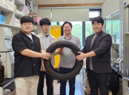
< (From left) Kyungmin Choi (MS-Ph.D. integrated course, Department of Chemistry), Dr. Beomsoon Park, Professor Soon Hyeok Hong, Dr. Kyoungil Cho >
Approximately 1.5 billions of tires are discarded globally every year, and this is identified as one of the major causes of serious environmental pollution. The research team at the Department of Chemistry at KAIST has achieved a breakthrough by selectively converting waste tires into high-purity cyclic alkenes, valuable chemical building blocks used in the production of rubber and nylon fibers. This advance marks a new milestone in chemical recycling technology for waste tires.
The team, led by Professor Soon Hyeok Hong, has developed a dual-catalyst-based reaction system that overcomes the long-standing challenges associated with recycling vulcanized rubber materials.
Tires are composed of complex blends of synthetic and natural rubber, and their physical strength and durability are reinforced with additives such as silica, carbon black, and antioxidants. In particular, cross-linking between rubber chains is formed through the vulcanization process, giving them a structure resistant to heat and pressure, which is one of the main reasons why chemical recycling of waste tires is difficult.
Until now, waste tire recycling has mainly relied on pyrolysis or mechanical recycling methods. The pyrolysis method is a technology that decomposes polymer chains at high temperatures of 350-800°C to convert them into fuel oil, but it clearly has limitations such as high energy consumption, low selectivity, and the production of low-quality hydrocarbon mixtures.
To solve these problems, the research team developed a method to convert waste rubber into useful chemicals using dual catalysis. The first catalyst helps to break down rubber molecules by changing their bonding structure, and the second catalyst creates cyclic compounds through a ring-closing reaction.
This process shows high selectivity of up to 92% and a yield of 82%. The produced cyclopentene can be recycled into rubber, and cyclohexene can be used as a raw material for nylon fibers, making them industrially very valuable.
The research team successfully applied the developed system to discarded waste tires, achieving selective conversion into high-purity cyclic alkenes. Unlike the existing pyrolysis method, this is evaluated as a new turning point in the field of waste tire recycling as it can produce high-value chemicals through low-temperature precision catalytic reactions.
In addition, this catalytic platform is compatible with a wide range of synthetic and waste rubbers, positioning it as a promising foundation for scalable, circular solutions in the polymer and materials industries.
< Figure 1. Development of a Catalytic Method for Chemical Recycling of Waste Rubber >
Professor Hong stated, "This research offers an innovative solution for the chemical recycling of waste tires. We aim to develop next-generation high-efficiency catalysts and lay the groundwork for commercialization to enhance economic feasibility. Ultimately, our goal is to contribute to solving the broader waste plastic problem through fundamental chemistry."
This research, in which Beomsoon Park, Kyoungil Cho, and Kyungmin Choi participated, was supported by the National Research Foundation of Korea and was published online in the internationally renowned academic journal ‘Chem’ on June 18th.
※Paper Title: Catalytic and Selective Chemical Recycling of Post-Consumer Rubbers into Cycloalkenes
※DOI: 10.1016/j.chempr.2025.102625
2025.06.26 View 581
New and Highly Efficient Recycling Technology to Turn Used Tires into Raw Materials for Rubber and Nylon
< (From left) Kyungmin Choi (MS-Ph.D. integrated course, Department of Chemistry), Dr. Beomsoon Park, Professor Soon Hyeok Hong, Dr. Kyoungil Cho >
Approximately 1.5 billions of tires are discarded globally every year, and this is identified as one of the major causes of serious environmental pollution. The research team at the Department of Chemistry at KAIST has achieved a breakthrough by selectively converting waste tires into high-purity cyclic alkenes, valuable chemical building blocks used in the production of rubber and nylon fibers. This advance marks a new milestone in chemical recycling technology for waste tires.
The team, led by Professor Soon Hyeok Hong, has developed a dual-catalyst-based reaction system that overcomes the long-standing challenges associated with recycling vulcanized rubber materials.
Tires are composed of complex blends of synthetic and natural rubber, and their physical strength and durability are reinforced with additives such as silica, carbon black, and antioxidants. In particular, cross-linking between rubber chains is formed through the vulcanization process, giving them a structure resistant to heat and pressure, which is one of the main reasons why chemical recycling of waste tires is difficult.
Until now, waste tire recycling has mainly relied on pyrolysis or mechanical recycling methods. The pyrolysis method is a technology that decomposes polymer chains at high temperatures of 350-800°C to convert them into fuel oil, but it clearly has limitations such as high energy consumption, low selectivity, and the production of low-quality hydrocarbon mixtures.
To solve these problems, the research team developed a method to convert waste rubber into useful chemicals using dual catalysis. The first catalyst helps to break down rubber molecules by changing their bonding structure, and the second catalyst creates cyclic compounds through a ring-closing reaction.
This process shows high selectivity of up to 92% and a yield of 82%. The produced cyclopentene can be recycled into rubber, and cyclohexene can be used as a raw material for nylon fibers, making them industrially very valuable.
The research team successfully applied the developed system to discarded waste tires, achieving selective conversion into high-purity cyclic alkenes. Unlike the existing pyrolysis method, this is evaluated as a new turning point in the field of waste tire recycling as it can produce high-value chemicals through low-temperature precision catalytic reactions.
In addition, this catalytic platform is compatible with a wide range of synthetic and waste rubbers, positioning it as a promising foundation for scalable, circular solutions in the polymer and materials industries.
< Figure 1. Development of a Catalytic Method for Chemical Recycling of Waste Rubber >
Professor Hong stated, "This research offers an innovative solution for the chemical recycling of waste tires. We aim to develop next-generation high-efficiency catalysts and lay the groundwork for commercialization to enhance economic feasibility. Ultimately, our goal is to contribute to solving the broader waste plastic problem through fundamental chemistry."
This research, in which Beomsoon Park, Kyoungil Cho, and Kyungmin Choi participated, was supported by the National Research Foundation of Korea and was published online in the internationally renowned academic journal ‘Chem’ on June 18th.
※Paper Title: Catalytic and Selective Chemical Recycling of Post-Consumer Rubbers into Cycloalkenes
※DOI: 10.1016/j.chempr.2025.102625
2025.06.26 View 581 -
 Military Combatants Usher in an Era of Personalized Training with New Materials
< Photo 1. (From left) Professor Steve Park of Materials Science and Engineering, Kyusoon Pak, Ph.D. Candidate (Army Major) >
Traditional military training often relies on standardized methods, which has limited the provision of optimized training tailored to individual combatants' characteristics or specific combat situations. To address this, our research team developed an e-textile platform, securing core technology that can reflect the unique traits of individual combatants and various combat scenarios. This technology has proven robust enough for battlefield use and is economical enough for widespread distribution to a large number of troops.
On June 25th, Professor Steve Park's research team at KAIST's Department of Materials Science and Engineering announced the development of a flexible, wearable electronic textile (E-textile) platform using an innovative technology that 'draws' electronic circuits directly onto fabric.
The wearable e-textile platform developed by the research team combines 3D printing technology with new materials engineering design to directly print flexible and highly durable sensors and electrodes onto textile substrates. This enables the collection of precise movement and human body data from individual combatants, which can then be used to propose customized training models.
Existing e-textile fabrication methods were often complex or limited in their ability to provide personalized customization. To overcome these challenges, the research team adopted an additive manufacturing technology called 'Direct Ink Writing (DIW)' 3D printing.
< Figure 1. Schematic diagram of e-textile manufactured with Direct Ink Writing (DIW) printing technology on various textiles, including combat uniforms >
This technology involves directly dispensing and printing special ink, which functions as sensors and electrodes, onto textile substrates in desired patterns. This allows for flexible implementation of various designs without the complex process of mask fabrication. This is expected to be an effective technology that can be easily supplied to hundreds of thousands of military personnel.
The core of this technology lies in the development of high-performance functional inks based on advanced materials engineering design. The research team combined styrene-butadiene-styrene (SBS) polymer, which provides flexibility, with multi-walled carbon nanotubes (MWCNT) for electrical conductivity. They developed a tensile/bending sensor ink that can stretch up to 102% and maintain stable performance even after 10,000 repetitive tests. This means that accurate data can be consistently obtained even during the strenuous movements of combatants.
< Figure 2. Measurement of human movement and breathing patterns using e-textile >
Furthermore, new material technology was applied to implement 'interconnect electrodes' that electrically connect the upper and lower layers of the fabric. The team developed an electrode ink combining silver (Ag) flakes with rigid polystyrene (PS) polymer, precisely controlling the impregnation level (how much the ink penetrates the fabric) to effectively connect both sides or multiple layers of the fabric. This secures the technology for producing multi-layered wearable electronic systems integrating sensors and electrodes.
< Figure 3. Experimental results of recognizing unknown objects after machine learning six objects using a smart glove >
The research team proved the platform's performance through actual human movement monitoring experiments. They printed the developed e-textile on major joint areas of clothing (shoulders, elbows, knees) and measured movements and posture changes during various exercises such as running, jumping jacks, and push-ups in real-time.
Additionally, they demonstrated the potential for applications such as monitoring breathing patterns using a smart mask and recognizing objects through machine learning and perceiving complex tactile information by printing multiple sensors and electrodes on gloves. These results show that the developed e-textile platform is effective in precisely understanding the movement dynamics of combatants.
This research is an important example demonstrating how cutting-edge new material technology can contribute to the advancement of the defense sector. Major Kyusoon Pak of the Army, who participated in this research, considered required objectives such as military applicability and economic feasibility for practical distribution from the research design stage.
< Figure 4. Experimental results showing that a multi-layered e-textile glove connected with interconnect electrodes can measure tensile/bending signals and pressure signals at a single point >
Major Pak stated, "Our military is currently facing both a crisis and an opportunity due to the decrease in military personnel resources caused by the demographic cliff and the advancement of science and technology. Also, respect for life in the battlefield is emerging as a significant issue. This research aims to secure original technology that can provide customized training according to military branch/duty and type of combat, thereby enhancing the combat power and ensuring the survivability of our soldiers."
He added, "I hope this research will be evaluated as a case that achieved both scientific contribution and military applicability."
This research, where Kyusoon Pak, Ph.D. Candidate (Army Major) from KAIST's Department of Materials Science and Engineering, participated as the first author and Professor Steve Park supervised, was published on May 27, 2025, in `npj Flexible Electronics (top 1.8% in JCR field)', an international academic journal in the electrical, electronic, and materials engineering fields.
* Paper Title: Fabrication of Multifunctional Wearable Interconnect E-textile Platform Using Direct Ink Writing (DIW) 3D Printing
* DOI: https://doi.org/10.1038/s41528-025-00414-7
This research was supported by the Ministry of Trade, Industry and Energy and the National Research Foundation of Korea.
2025.06.25 View 237
Military Combatants Usher in an Era of Personalized Training with New Materials
< Photo 1. (From left) Professor Steve Park of Materials Science and Engineering, Kyusoon Pak, Ph.D. Candidate (Army Major) >
Traditional military training often relies on standardized methods, which has limited the provision of optimized training tailored to individual combatants' characteristics or specific combat situations. To address this, our research team developed an e-textile platform, securing core technology that can reflect the unique traits of individual combatants and various combat scenarios. This technology has proven robust enough for battlefield use and is economical enough for widespread distribution to a large number of troops.
On June 25th, Professor Steve Park's research team at KAIST's Department of Materials Science and Engineering announced the development of a flexible, wearable electronic textile (E-textile) platform using an innovative technology that 'draws' electronic circuits directly onto fabric.
The wearable e-textile platform developed by the research team combines 3D printing technology with new materials engineering design to directly print flexible and highly durable sensors and electrodes onto textile substrates. This enables the collection of precise movement and human body data from individual combatants, which can then be used to propose customized training models.
Existing e-textile fabrication methods were often complex or limited in their ability to provide personalized customization. To overcome these challenges, the research team adopted an additive manufacturing technology called 'Direct Ink Writing (DIW)' 3D printing.
< Figure 1. Schematic diagram of e-textile manufactured with Direct Ink Writing (DIW) printing technology on various textiles, including combat uniforms >
This technology involves directly dispensing and printing special ink, which functions as sensors and electrodes, onto textile substrates in desired patterns. This allows for flexible implementation of various designs without the complex process of mask fabrication. This is expected to be an effective technology that can be easily supplied to hundreds of thousands of military personnel.
The core of this technology lies in the development of high-performance functional inks based on advanced materials engineering design. The research team combined styrene-butadiene-styrene (SBS) polymer, which provides flexibility, with multi-walled carbon nanotubes (MWCNT) for electrical conductivity. They developed a tensile/bending sensor ink that can stretch up to 102% and maintain stable performance even after 10,000 repetitive tests. This means that accurate data can be consistently obtained even during the strenuous movements of combatants.
< Figure 2. Measurement of human movement and breathing patterns using e-textile >
Furthermore, new material technology was applied to implement 'interconnect electrodes' that electrically connect the upper and lower layers of the fabric. The team developed an electrode ink combining silver (Ag) flakes with rigid polystyrene (PS) polymer, precisely controlling the impregnation level (how much the ink penetrates the fabric) to effectively connect both sides or multiple layers of the fabric. This secures the technology for producing multi-layered wearable electronic systems integrating sensors and electrodes.
< Figure 3. Experimental results of recognizing unknown objects after machine learning six objects using a smart glove >
The research team proved the platform's performance through actual human movement monitoring experiments. They printed the developed e-textile on major joint areas of clothing (shoulders, elbows, knees) and measured movements and posture changes during various exercises such as running, jumping jacks, and push-ups in real-time.
Additionally, they demonstrated the potential for applications such as monitoring breathing patterns using a smart mask and recognizing objects through machine learning and perceiving complex tactile information by printing multiple sensors and electrodes on gloves. These results show that the developed e-textile platform is effective in precisely understanding the movement dynamics of combatants.
This research is an important example demonstrating how cutting-edge new material technology can contribute to the advancement of the defense sector. Major Kyusoon Pak of the Army, who participated in this research, considered required objectives such as military applicability and economic feasibility for practical distribution from the research design stage.
< Figure 4. Experimental results showing that a multi-layered e-textile glove connected with interconnect electrodes can measure tensile/bending signals and pressure signals at a single point >
Major Pak stated, "Our military is currently facing both a crisis and an opportunity due to the decrease in military personnel resources caused by the demographic cliff and the advancement of science and technology. Also, respect for life in the battlefield is emerging as a significant issue. This research aims to secure original technology that can provide customized training according to military branch/duty and type of combat, thereby enhancing the combat power and ensuring the survivability of our soldiers."
He added, "I hope this research will be evaluated as a case that achieved both scientific contribution and military applicability."
This research, where Kyusoon Pak, Ph.D. Candidate (Army Major) from KAIST's Department of Materials Science and Engineering, participated as the first author and Professor Steve Park supervised, was published on May 27, 2025, in `npj Flexible Electronics (top 1.8% in JCR field)', an international academic journal in the electrical, electronic, and materials engineering fields.
* Paper Title: Fabrication of Multifunctional Wearable Interconnect E-textile Platform Using Direct Ink Writing (DIW) 3D Printing
* DOI: https://doi.org/10.1038/s41528-025-00414-7
This research was supported by the Ministry of Trade, Industry and Energy and the National Research Foundation of Korea.
2025.06.25 View 237 -
 KAIST's Li-Fi - Achieves 100 Times Faster Speed and Enhanced Security of Wi-Fi
- KAIST-KRISS Develop 'On-Device Encryption Optical Transmitter' Based on Eco-Friendly Quantum Dots
- New Li-Fi Platform Technology Achieves High Performance with 17.4% Device Efficiency and 29,000 nit Brightness, Simultaneously Improving Transmission Speed and Security
- Presents New Methodology for High-Speed and Encrypted Communication Through Single-Device-Based Dual-Channel Optical Modulation
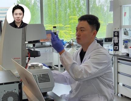
< Photo 1. (Front row from left) Seungmin Shin, First Author; Professor Himchan Cho; (Back row from left) Hyungdoh Lee, Seungwoo Lee, Wonbeom Lee; (Top left) Dr. Kyung-geun Lim >
Li-Fi (Light Fidelity) is a wireless communication technology that utilizes the visible light spectrum (400-800 THz), similar to LED light, offering speeds up to 100 times faster than existing Wi-Fi (up to 224 Gbps). While it has fewer limitations in available frequency allocation and less radio interference, it is relatively vulnerable to security breaches as anyone can access it. Korean researchers have now proposed a new Li-Fi platform that overcomes the limitations of conventional optical communication devices and can simultaneously enhance both transmission speed and security.
KAIST (President Kwang Hyung Lee) announced on the 24th that Professor Himchan Cho's research team from the Department of Materials Science and Engineering, in collaboration with Dr. Kyung-geun Lim of the Korea Research Institute of Standards and Science (KRISS, President Ho-Seong Lee) under the National Research Council of Science & Technology (NST, Chairman Young-Sik Kim), has developed 'on-device encryption optical communication device' technology for the utilization of 'Li-Fi,' which is attracting attention as a next-generation ultra-high-speed data communication.
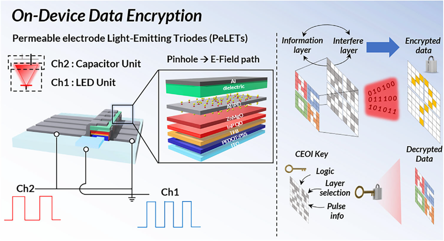
Professor Cho's team created high-efficiency light-emitting triode devices using eco-friendly quantum dots (low-toxicity and sustainable materials). The device developed by the research team is a mechanism that generates light using an electric field. Specifically, the electric field is concentrated in 'tiny holes (pinholes) in the permeable electrode' and transmitted beyond the electrode. This device utilizes this principle to simultaneously process two input data streams.
Using this principle, the research team developed a technology called 'on-device encryption optical transmitter.' The core of this technology is that the device itself converts information into light and simultaneously encrypts it. This means that enhanced security data transmission is possible without the need for complex, separate equipment.
External Quantum Efficiency (EQE) is an indicator of how efficiently electricity is converted into light, with a general commercialization standard of about 20%. The newly developed device recorded an EQE of 17.4%, and its luminance was 29,000 nit, significantly exceeding the maximum brightness of a smartphone OLED screen, which is 2,000 nit, demonstrating a brightness more than 10 times higher.
< Figure 1. Schematic diagram of the device structure developed by the research team and encrypted communication >
Furthermore, to more accurately understand how this device converts information into light, the research team used a method called 'transient electroluminescence analysis.' They analyzed the light-emitting characteristics generated by the device when voltage was instantaneously applied for very short durations (hundreds of nanoseconds = billionths of a second). Through this analysis, they investigated the movement of charges within the device at hundreds of nanoseconds, elucidating the operating mechanism of dual-channel optical modulation implemented within a single device.
Professor Himchan Cho of KAIST stated, "This research overcomes the limitations of existing optical communication devices and proposes a new communication platform that can both increase transmission speed and enhance security."
< Photo 2. Professor Himchan Cho, Department of Materials Science and Engineering >
He added, "This technology, which strengthens security without additional equipment and simultaneously enables encryption and transmission, can be widely applied in various fields where security is crucial in the future."
This research, with Seungmin Shin, a Ph.D. candidate at KAIST's Department of Materials Science and Engineering, participating as the first author, and Professor Himchan Cho and Dr. Kyung-geun Lim of KRISS as co-corresponding authors, was published in the international journal 'Advanced Materials' on May 30th and was selected as an inside front cover paper.※ Paper Title: High-Efficiency Quantum Dot Permeable electrode Light-Emitting Triodes for Visible-Light Communications and On-Device Data Encryption※ DOI: https://doi.org/10.1002/adma.202503189
This research was supported by the National Research Foundation of Korea, the National Research Council of Science & Technology (NST), and the Korea Institute for Advancement of Technology.
2025.06.24 View 703
KAIST's Li-Fi - Achieves 100 Times Faster Speed and Enhanced Security of Wi-Fi
- KAIST-KRISS Develop 'On-Device Encryption Optical Transmitter' Based on Eco-Friendly Quantum Dots
- New Li-Fi Platform Technology Achieves High Performance with 17.4% Device Efficiency and 29,000 nit Brightness, Simultaneously Improving Transmission Speed and Security
- Presents New Methodology for High-Speed and Encrypted Communication Through Single-Device-Based Dual-Channel Optical Modulation
< Photo 1. (Front row from left) Seungmin Shin, First Author; Professor Himchan Cho; (Back row from left) Hyungdoh Lee, Seungwoo Lee, Wonbeom Lee; (Top left) Dr. Kyung-geun Lim >
Li-Fi (Light Fidelity) is a wireless communication technology that utilizes the visible light spectrum (400-800 THz), similar to LED light, offering speeds up to 100 times faster than existing Wi-Fi (up to 224 Gbps). While it has fewer limitations in available frequency allocation and less radio interference, it is relatively vulnerable to security breaches as anyone can access it. Korean researchers have now proposed a new Li-Fi platform that overcomes the limitations of conventional optical communication devices and can simultaneously enhance both transmission speed and security.
KAIST (President Kwang Hyung Lee) announced on the 24th that Professor Himchan Cho's research team from the Department of Materials Science and Engineering, in collaboration with Dr. Kyung-geun Lim of the Korea Research Institute of Standards and Science (KRISS, President Ho-Seong Lee) under the National Research Council of Science & Technology (NST, Chairman Young-Sik Kim), has developed 'on-device encryption optical communication device' technology for the utilization of 'Li-Fi,' which is attracting attention as a next-generation ultra-high-speed data communication.
Professor Cho's team created high-efficiency light-emitting triode devices using eco-friendly quantum dots (low-toxicity and sustainable materials). The device developed by the research team is a mechanism that generates light using an electric field. Specifically, the electric field is concentrated in 'tiny holes (pinholes) in the permeable electrode' and transmitted beyond the electrode. This device utilizes this principle to simultaneously process two input data streams.
Using this principle, the research team developed a technology called 'on-device encryption optical transmitter.' The core of this technology is that the device itself converts information into light and simultaneously encrypts it. This means that enhanced security data transmission is possible without the need for complex, separate equipment.
External Quantum Efficiency (EQE) is an indicator of how efficiently electricity is converted into light, with a general commercialization standard of about 20%. The newly developed device recorded an EQE of 17.4%, and its luminance was 29,000 nit, significantly exceeding the maximum brightness of a smartphone OLED screen, which is 2,000 nit, demonstrating a brightness more than 10 times higher.
< Figure 1. Schematic diagram of the device structure developed by the research team and encrypted communication >
Furthermore, to more accurately understand how this device converts information into light, the research team used a method called 'transient electroluminescence analysis.' They analyzed the light-emitting characteristics generated by the device when voltage was instantaneously applied for very short durations (hundreds of nanoseconds = billionths of a second). Through this analysis, they investigated the movement of charges within the device at hundreds of nanoseconds, elucidating the operating mechanism of dual-channel optical modulation implemented within a single device.
Professor Himchan Cho of KAIST stated, "This research overcomes the limitations of existing optical communication devices and proposes a new communication platform that can both increase transmission speed and enhance security."
< Photo 2. Professor Himchan Cho, Department of Materials Science and Engineering >
He added, "This technology, which strengthens security without additional equipment and simultaneously enables encryption and transmission, can be widely applied in various fields where security is crucial in the future."
This research, with Seungmin Shin, a Ph.D. candidate at KAIST's Department of Materials Science and Engineering, participating as the first author, and Professor Himchan Cho and Dr. Kyung-geun Lim of KRISS as co-corresponding authors, was published in the international journal 'Advanced Materials' on May 30th and was selected as an inside front cover paper.※ Paper Title: High-Efficiency Quantum Dot Permeable electrode Light-Emitting Triodes for Visible-Light Communications and On-Device Data Encryption※ DOI: https://doi.org/10.1002/adma.202503189
This research was supported by the National Research Foundation of Korea, the National Research Council of Science & Technology (NST), and the Korea Institute for Advancement of Technology.
2025.06.24 View 703 -
 KAIST Develops Customized Tactile Sensor That Can Detect Light Breath, Pressure and Sound
< Photo 1. (From left) Professor Inkyu Park of KAIST Department of Mechanical Engineering (ME), Dr. Jungrak Choi of ETRI, Ph.D. Candidate Donho Lee and M.S. Graduate Chankyu Han of KAIST ME >
When a robot grabs an object or a medical device detects a pulse, the tactile sensor is the technology that senses pressure like a fingertip. Existing sensors had disadvantages, such as slow responses or declining accuracy after repeated use, but Korean researchers have succeeded in developing a sensor that can quickly and accurately detect even light breath, pressure, and sound. This sensor can be used across a broad range — from everyday movements to medical diagnostics.
KAIST (represented by President Kwang Hyung Lee) announced on the 23rd of June that Professor Inkyu Park’s team from the Department of Mechanical Engineering, through a collaborative research project with the Electronics and Telecommunications Research Institute (ETRI, President Seung Chan Bang ) under the National Research Council of Science & Technology (NST, Chairman Young Sik Kim), has developed an innovative technology that overcomes the structural limitations of existing tactile sensors.
The core of this joint research is the implementation of a customized tactile sensor that simultaneously achieves flexibility, precision, and repeatable durability by applying Thermoformed 3D Electronics (T3DE).
< Figure 1. Comparative evaluation of soft elastomer–based 3D structure versus thermoforming-based 3D structure in terms of mechanical properties. >
In particular, soft elastomer-based sensors (rubber, silicone, etc. — materials that stretch and return to their original shape) have structural problems such as slow response times, high hysteresis*, and creep**, but this new platform operates precisely in diverse environments and overcomes these limitations.
*Hysteresis: A phenomenon where the previously applied force or change is retained like a “memory,” so that the same stimulus does not always produce the same result.
**Creep: The phenomenon where a material slowly deforms when a force is continuously applied.
T3DE sensors are manufactured by precisely forming electrodes on a 2D film, then thermoforming them into a 3D structure under heat and pressure. Specifically, the top electrodes and supporting pillar structures of the sensor are designed to allow the fine-tuning of the mechanical properties for different purposes. By adjusting microstructural parameters — such as the thickness, length, and number of support pillars — the sensor’s Young’s modulus* can be tuned across a broad range of 10 Pa to 1 MPa. This matches the stiffness of biological tissues like skin, muscle, and tendons, making them highly suitable as bio-interface sensors.
*Young’s modulus: An index representing a material's stiffness; this research can control this index to match various biological tissues.
The newly developed T3DE sensor uses air as a dielectric material to reduce power consumption and demonstrates outstanding performance in sensitivity, response time, thermal stability, and repeatable accuracy.
Experimental results showed that the sensor achieved △sensitivity of 5,884 kPa⁻¹, △response time of 0.1 ms (less than one-thousandth of a second), △hysteresis of less than 0.5%, and maintained a repeatable precision of 99.9% or higher even after 5,000 repeated measurements.
< Figure 2. Graphic Overview of thermoformed 3D electronics (T3DE) >
The research team also constructed a high-resolution 40×70 array, comprising a total of 2,800 densely packed sensors, to visualize the pressure distribution on the sole of the foot in real time during exercise and confirmed the possibility of using the sensor for wrist pulse measurement to assess vascular health. Furthermore, successful results were also achieved in sound-detection experiments at a level comparable to commercial acoustic sensors. In short, the sensor can precisely and quickly measure foot pressure, pulse, and sound, allowing it to be applied in areas such as sports, health, and sound sensing.
The T3DE technology was also applied to an augmented-reality(AR)-based surgical training system. By adjusting the stiffness of each sensor element to match that of biological tissues, the system provided real-time visual and tactile feedback according to the pressure applied during surgical incisions. It also offered real-time warnings if an incision was too deep or approached a risky area, making it a promising technology for enhancing immersion and accuracy in medical training.
KAIST Professor Inkyu Park stated, “Because this sensor can be precisely tuned from the design stage and operates reliably across diverse environments, it can be used not only in everyday life, but also in a variety of fields such as healthcare, rehabilitation, and virtual reality.”
The research was co-led as first authors by Dr. Jungrak Choi of ETRI, KAIST master’s student Chankyu Han, and Ph.D. candidate Donho Lee, under the overall guidance of Professor Inkyu Park. The research results were published in the May 2025 issue of ‘Science Advances’ and introduced to the global research community through the journal’s official SNS channels (Facebook, Twitter).
※ Thesis Title: Thermoforming 2D films into 3D electronics for high-performance, customizable tactile sensing
※ DOI: 10.1126/sciadv.adv0057
< Figure 3. The introduction of the study on the official SNS posting by Science Advances >
This research was supported by the Ministry of Trade, Industry and Energy, the National Research Foundation of Korea, and the Korea Institute for Advancement of Technology.
2025.06.23 View 402
KAIST Develops Customized Tactile Sensor That Can Detect Light Breath, Pressure and Sound
< Photo 1. (From left) Professor Inkyu Park of KAIST Department of Mechanical Engineering (ME), Dr. Jungrak Choi of ETRI, Ph.D. Candidate Donho Lee and M.S. Graduate Chankyu Han of KAIST ME >
When a robot grabs an object or a medical device detects a pulse, the tactile sensor is the technology that senses pressure like a fingertip. Existing sensors had disadvantages, such as slow responses or declining accuracy after repeated use, but Korean researchers have succeeded in developing a sensor that can quickly and accurately detect even light breath, pressure, and sound. This sensor can be used across a broad range — from everyday movements to medical diagnostics.
KAIST (represented by President Kwang Hyung Lee) announced on the 23rd of June that Professor Inkyu Park’s team from the Department of Mechanical Engineering, through a collaborative research project with the Electronics and Telecommunications Research Institute (ETRI, President Seung Chan Bang ) under the National Research Council of Science & Technology (NST, Chairman Young Sik Kim), has developed an innovative technology that overcomes the structural limitations of existing tactile sensors.
The core of this joint research is the implementation of a customized tactile sensor that simultaneously achieves flexibility, precision, and repeatable durability by applying Thermoformed 3D Electronics (T3DE).
< Figure 1. Comparative evaluation of soft elastomer–based 3D structure versus thermoforming-based 3D structure in terms of mechanical properties. >
In particular, soft elastomer-based sensors (rubber, silicone, etc. — materials that stretch and return to their original shape) have structural problems such as slow response times, high hysteresis*, and creep**, but this new platform operates precisely in diverse environments and overcomes these limitations.
*Hysteresis: A phenomenon where the previously applied force or change is retained like a “memory,” so that the same stimulus does not always produce the same result.
**Creep: The phenomenon where a material slowly deforms when a force is continuously applied.
T3DE sensors are manufactured by precisely forming electrodes on a 2D film, then thermoforming them into a 3D structure under heat and pressure. Specifically, the top electrodes and supporting pillar structures of the sensor are designed to allow the fine-tuning of the mechanical properties for different purposes. By adjusting microstructural parameters — such as the thickness, length, and number of support pillars — the sensor’s Young’s modulus* can be tuned across a broad range of 10 Pa to 1 MPa. This matches the stiffness of biological tissues like skin, muscle, and tendons, making them highly suitable as bio-interface sensors.
*Young’s modulus: An index representing a material's stiffness; this research can control this index to match various biological tissues.
The newly developed T3DE sensor uses air as a dielectric material to reduce power consumption and demonstrates outstanding performance in sensitivity, response time, thermal stability, and repeatable accuracy.
Experimental results showed that the sensor achieved △sensitivity of 5,884 kPa⁻¹, △response time of 0.1 ms (less than one-thousandth of a second), △hysteresis of less than 0.5%, and maintained a repeatable precision of 99.9% or higher even after 5,000 repeated measurements.
< Figure 2. Graphic Overview of thermoformed 3D electronics (T3DE) >
The research team also constructed a high-resolution 40×70 array, comprising a total of 2,800 densely packed sensors, to visualize the pressure distribution on the sole of the foot in real time during exercise and confirmed the possibility of using the sensor for wrist pulse measurement to assess vascular health. Furthermore, successful results were also achieved in sound-detection experiments at a level comparable to commercial acoustic sensors. In short, the sensor can precisely and quickly measure foot pressure, pulse, and sound, allowing it to be applied in areas such as sports, health, and sound sensing.
The T3DE technology was also applied to an augmented-reality(AR)-based surgical training system. By adjusting the stiffness of each sensor element to match that of biological tissues, the system provided real-time visual and tactile feedback according to the pressure applied during surgical incisions. It also offered real-time warnings if an incision was too deep or approached a risky area, making it a promising technology for enhancing immersion and accuracy in medical training.
KAIST Professor Inkyu Park stated, “Because this sensor can be precisely tuned from the design stage and operates reliably across diverse environments, it can be used not only in everyday life, but also in a variety of fields such as healthcare, rehabilitation, and virtual reality.”
The research was co-led as first authors by Dr. Jungrak Choi of ETRI, KAIST master’s student Chankyu Han, and Ph.D. candidate Donho Lee, under the overall guidance of Professor Inkyu Park. The research results were published in the May 2025 issue of ‘Science Advances’ and introduced to the global research community through the journal’s official SNS channels (Facebook, Twitter).
※ Thesis Title: Thermoforming 2D films into 3D electronics for high-performance, customizable tactile sensing
※ DOI: 10.1126/sciadv.adv0057
< Figure 3. The introduction of the study on the official SNS posting by Science Advances >
This research was supported by the Ministry of Trade, Industry and Energy, the National Research Foundation of Korea, and the Korea Institute for Advancement of Technology.
2025.06.23 View 402 -
 KAIST Researchers Unveil an AI that Generates "Unexpectedly Original" Designs
< Photo 1. Professor Jaesik Choi, KAIST Kim Jaechul Graduate School of AI >
Recently, text-based image generation models can automatically create high-resolution, high-quality images solely from natural language descriptions. However, when a typical example like the Stable Diffusion model is given the text "creative," its ability to generate truly creative images remains limited. KAIST researchers have developed a technology that can enhance the creativity of text-based image generation models such as Stable Diffusion without additional training, allowing AI to draw creative chair designs that are far from ordinary.
Professor Jaesik Choi's research team at KAIST Kim Jaechul Graduate School of AI, in collaboration with NAVER AI Lab, developed this technology to enhance the creative generation of AI generative models without the need for additional training.
< Photo 2. Gayoung Lee, Researcher at NAVER AI Lab; Dahee Kwon, Ph.D. Candidate at KAIST Kim Jaechul Graduate School of AI; Jiyeon Han, Ph.D. Candidate at KAIST Kim Jaechul Graduate School of AI; Junho Kim, Researcher at NAVER AI Lab >
Professor Choi's research team developed a technology to enhance creative generation by amplifying the internal feature maps of text-based image generation models. They also discovered that shallow blocks within the model play a crucial role in creative generation. They confirmed that amplifying values in the high-frequency region after converting feature maps to the frequency domain can lead to noise or fragmented color patterns. Accordingly, the research team demonstrated that amplifying the low-frequency region of shallow blocks can effectively enhance creative generation.
Considering originality and usefulness as two key elements defining creativity, the research team proposed an algorithm that automatically selects the optimal amplification value for each block within the generative model.
Through the developed algorithm, appropriate amplification of the internal feature maps of a pre-trained Stable Diffusion model was able to enhance creative generation without additional classification data or training.
< Figure 1. Overview of the methodology researched by the development team. After converting the internal feature map of a pre-trained generative model into the frequency domain through Fast Fourier Transform, the low-frequency region of the feature map is amplified, then re-transformed into the feature space via Inverse Fast Fourier Transform to generate an image. >
The research team quantitatively proved, using various metrics, that their developed algorithm can generate images that are more novel than those from existing models, without significantly compromising utility.
In particular, they confirmed an increase in image diversity by mitigating the mode collapse problem that occurs in the SDXL-Turbo model, which was developed to significantly improve the image generation speed of the Stable Diffusion XL (SDXL) model. Furthermore, user studies showed that human evaluation also confirmed a significant improvement in novelty relative to utility compared to existing methods.
Jiyeon Han and Dahee Kwon, Ph.D. candidates at KAIST and co-first authors of the paper, stated, "This is the first methodology to enhance the creative generation of generative models without new training or fine-tuning. We have shown that the latent creativity within trained AI generative models can be enhanced through feature map manipulation."
They added, "This research makes it easy to generate creative images using only text from existing trained models. It is expected to provide new inspiration in various fields, such as creative product design, and contribute to the practical and useful application of AI models in the creative ecosystem."
< Figure 2. Application examples of the methodology researched by the development team. Various Stable Diffusion models generate novel images compared to existing generations while maintaining the meaning of the generated object. >
This research, co-authored by Jiyeon Han and Dahee Kwon, Ph.D. candidates at KAIST Kim Jaechul Graduate School of AI, was presented on June 16 at the International Conference on Computer Vision and Pattern Recognition (CVPR), an international academic conference.* Paper Title: Enhancing Creative Generation on Stable Diffusion-based Models* DOI: https://doi.org/10.48550/arXiv.2503.23538
This research was supported by the KAIST-NAVER Ultra-creative AI Research Center, the Innovation Growth Engine Project Explainable AI, the AI Research Hub Project, and research on flexible evolving AI technology development in line with increasingly strengthened ethical policies, all funded by the Ministry of Science and ICT through the Institute for Information & Communications Technology Promotion. It also received support from the KAIST AI Graduate School Program and was carried out at the KAIST Future Defense AI Specialized Research Center with support from the Defense Acquisition Program Administration and the Agency for Defense Development.
2025.06.20 View 660
KAIST Researchers Unveil an AI that Generates "Unexpectedly Original" Designs
< Photo 1. Professor Jaesik Choi, KAIST Kim Jaechul Graduate School of AI >
Recently, text-based image generation models can automatically create high-resolution, high-quality images solely from natural language descriptions. However, when a typical example like the Stable Diffusion model is given the text "creative," its ability to generate truly creative images remains limited. KAIST researchers have developed a technology that can enhance the creativity of text-based image generation models such as Stable Diffusion without additional training, allowing AI to draw creative chair designs that are far from ordinary.
Professor Jaesik Choi's research team at KAIST Kim Jaechul Graduate School of AI, in collaboration with NAVER AI Lab, developed this technology to enhance the creative generation of AI generative models without the need for additional training.
< Photo 2. Gayoung Lee, Researcher at NAVER AI Lab; Dahee Kwon, Ph.D. Candidate at KAIST Kim Jaechul Graduate School of AI; Jiyeon Han, Ph.D. Candidate at KAIST Kim Jaechul Graduate School of AI; Junho Kim, Researcher at NAVER AI Lab >
Professor Choi's research team developed a technology to enhance creative generation by amplifying the internal feature maps of text-based image generation models. They also discovered that shallow blocks within the model play a crucial role in creative generation. They confirmed that amplifying values in the high-frequency region after converting feature maps to the frequency domain can lead to noise or fragmented color patterns. Accordingly, the research team demonstrated that amplifying the low-frequency region of shallow blocks can effectively enhance creative generation.
Considering originality and usefulness as two key elements defining creativity, the research team proposed an algorithm that automatically selects the optimal amplification value for each block within the generative model.
Through the developed algorithm, appropriate amplification of the internal feature maps of a pre-trained Stable Diffusion model was able to enhance creative generation without additional classification data or training.
< Figure 1. Overview of the methodology researched by the development team. After converting the internal feature map of a pre-trained generative model into the frequency domain through Fast Fourier Transform, the low-frequency region of the feature map is amplified, then re-transformed into the feature space via Inverse Fast Fourier Transform to generate an image. >
The research team quantitatively proved, using various metrics, that their developed algorithm can generate images that are more novel than those from existing models, without significantly compromising utility.
In particular, they confirmed an increase in image diversity by mitigating the mode collapse problem that occurs in the SDXL-Turbo model, which was developed to significantly improve the image generation speed of the Stable Diffusion XL (SDXL) model. Furthermore, user studies showed that human evaluation also confirmed a significant improvement in novelty relative to utility compared to existing methods.
Jiyeon Han and Dahee Kwon, Ph.D. candidates at KAIST and co-first authors of the paper, stated, "This is the first methodology to enhance the creative generation of generative models without new training or fine-tuning. We have shown that the latent creativity within trained AI generative models can be enhanced through feature map manipulation."
They added, "This research makes it easy to generate creative images using only text from existing trained models. It is expected to provide new inspiration in various fields, such as creative product design, and contribute to the practical and useful application of AI models in the creative ecosystem."
< Figure 2. Application examples of the methodology researched by the development team. Various Stable Diffusion models generate novel images compared to existing generations while maintaining the meaning of the generated object. >
This research, co-authored by Jiyeon Han and Dahee Kwon, Ph.D. candidates at KAIST Kim Jaechul Graduate School of AI, was presented on June 16 at the International Conference on Computer Vision and Pattern Recognition (CVPR), an international academic conference.* Paper Title: Enhancing Creative Generation on Stable Diffusion-based Models* DOI: https://doi.org/10.48550/arXiv.2503.23538
This research was supported by the KAIST-NAVER Ultra-creative AI Research Center, the Innovation Growth Engine Project Explainable AI, the AI Research Hub Project, and research on flexible evolving AI technology development in line with increasingly strengthened ethical policies, all funded by the Ministry of Science and ICT through the Institute for Information & Communications Technology Promotion. It also received support from the KAIST AI Graduate School Program and was carried out at the KAIST Future Defense AI Specialized Research Center with support from the Defense Acquisition Program Administration and the Agency for Defense Development.
2025.06.20 View 660 -
 KAIST Develops Glare-Free, Heat-Blocking 'Smart Window'... Applicable to Buildings and Vehicles
• Professor Hong Chul Moon of the Department of Chemical and Biomolecular Engineering develops RECM, a next-generation smart window technology, expecting cooling energy savings and effective indoor thermal management.
• When using the developed RECM, a significantly superior temperature reduction effect is observed compared to conventional windows.
• With a 'pedestrian-friendly smart window' design that eliminates glare by suppressing external reflections, it is expected to be adapted in architectural structures, transportation, and more.
< (From left) First author Hoy Jung Jo, Professor Hong Chul Moon >
In the building sector, which accounts for approximately 40% of global energy consumption, heat ingress through windows has been identified as a primary cause of wasted heating and cooling energy. Our research team has successfully developed a 'pedestrian-friendly smart window' technology capable of not only reducing heating and cooling energy in urban buildings but also resolving the persistent issue of 'light pollution' in urban living.
On the 17th of June, Professor Hong Chul Moon's research team at KAIST's Department of Chemical and Biomolecular Engineering announced the development of a 'smart window technology' that allows users to control the light and heat entering through windows according to their intent, and effectively neutralize glare from external sources.
Recently, 'active smart window' technology, which enables free adjustment of light and heat based on user operation, has garnered significant attention. Unlike conventional windows that passively react to changes in temperature or light, this is a next-generation window system that can be controlled in real-time via electrical signals.
The next-generation smart window technology developed by the research team, RECM (Reversible Electrodeposition and Electrochromic Mirror), is a smart window system based on a single-structured *electrochromic device that can actively control the transmittance of visible light and near-infrared (heat).
*Electrochromic device: A device whose optical properties change in response to an electrical signal.
In particular, by effectively suppressing the glare phenomenon caused by external reflected light—a problem previously identified in traditional metal *deposition smart windows—through the combined application of electrochromic materials, a 'pedestrian-friendly smart window' suitable for building facades has been realized.
*Deposition: A process involving the electrochemical reaction to coat metal ions, such as Ag+, onto an electrode surface in solid form.
The RECM system developed in this study operates in three modes depending on voltage control.
Mode I (Transparent Mode) is advantageous for allowing sunlight to enter the indoor space during winter, as it transmits both light and heat like ordinary glass.
In Mode II (Colored Mode), *Prussian Blue (PB) and **DHV+• chemical species are formed through a redox (oxidation-reduction) reaction, causing the window to turn a deep blue color. In this state, light is absorbed, and only a portion of the heat is transmitted, allowing for privacy while enabling appropriate indoor temperature control.
*Prussian Blue: An electrochromic material that transitions between colorless and blue upon electrical stimulation.
**DHV+•: A radical state colored molecule generated upon electrical stimulation.
Mode III (Colored and Deposition Mode) involves the reduction and deposition of silver (Ag+) ions on the electrode surface, reflecting both light and heat. Concurrently, the colored material absorbs the reflected light, effectively blocking glare for external pedestrians.
The research team validated the practical indoor temperature reduction effect of the RECM technology through experiments utilizing a miniature model house. When a conventional glass window was installed, the indoor temperature rose to 58.7°C within 45 minutes. Conversely, when RECM was operated in Mode III, the temperature reached 31.5°C, demonstrating a temperature reduction effect of approximately 27.2°C.
Furthermore, since each state transition is achievable solely by electrical signals, it is regarded as an active smart technology capable of instantaneous response according to season, time, and intended use.
< Figure 1. Operation mechanism of the RECM smart window. The RECM system can switch among three states—transparent, colored, and colored & deposition—via electrical stimulation. At -1.6 V, DHV•+ and Prussian Blue (PB) are formed, blocking visible light to provide privacy protection and heat blocking. At -2.0 V, silver (Ag) is deposited on the electrode surface, reflecting light and heat, while DHV•+ and Prussian Blue absorb reflected light, effectively suppressing external glare. Through this mechanism, it functions as an active smart window that simultaneously controls light, heat, and glare. >
Professor Hong Chul Moon of KAIST, the corresponding author of this study, stated, "This research goes beyond existing smart window technologies limited to visible light control, presenting a truly smart window platform that comprehensively considers not only active indoor thermal control but also the visual safety of pedestrians." He added, "Various applications are anticipated, from urban buildings to vehicles and trains."
< Figure 2. Analysis of glare suppression effect of conventional reflective smart windows and RECM. This figure presents the results comparing the glare phenomenon occurring during silver (Ag) deposition between conventional reflective smart windows and RECM Mode III. Conventional reflective devices resulted in strong reflected light on the desk surface due to their high reflectivity. In contrast, RECM Mode III, where the colored material absorbed reflected light, showed a 33% reduction in reflected light intensity, and no reflected light was observed from outside. This highlights the RECM system's distinctiveness and practicality as a 'pedestrian-friendly smart window' optimized for dense urban environments, extending beyond just heat blocking. >
The findings of this research were published on June 13, 2025, in Volume 10, Issue 6 of 'ACS Energy Letters'. The listed authors for this publication are Hoy Jung Jo, Yeon Jae Jang, Hyeon-Don Kim, Kwang-Seop Kim, and Hong Chul Moon.
※ Paper Title: Glare-Free, Energy-Efficient Smart Windows: A Pedestrian-Friendly System with Dynamically Tunable Light and Heat Regulation
※ DOI: 10.1021/acsenergylett.5c00637
< Figure 3. Temperature reduction performance verification in a miniature model house. The actual heat blocking effect was evaluated by applying RECM devices to a model building. Under identical conditions, the indoor temperature with ordinary glass rose to 58.7°C, whereas with RECM in Mode III, it reached 31.5°C, demonstrating a maximum temperature reduction effect of 27.2°C. The indoor temperature difference was also visually confirmed through thermal images, which proves the potential for indoor temperature control in urban buildings. >
This research was supported by the Nano & Material Technology Development Program through the National Research Foundation of Korea (NRF) funded by the Ministry of Science and ICT and the internal research program of the Korea Institute of Machinery and Materials.
2025.06.20 View 2023
KAIST Develops Glare-Free, Heat-Blocking 'Smart Window'... Applicable to Buildings and Vehicles
• Professor Hong Chul Moon of the Department of Chemical and Biomolecular Engineering develops RECM, a next-generation smart window technology, expecting cooling energy savings and effective indoor thermal management.
• When using the developed RECM, a significantly superior temperature reduction effect is observed compared to conventional windows.
• With a 'pedestrian-friendly smart window' design that eliminates glare by suppressing external reflections, it is expected to be adapted in architectural structures, transportation, and more.
< (From left) First author Hoy Jung Jo, Professor Hong Chul Moon >
In the building sector, which accounts for approximately 40% of global energy consumption, heat ingress through windows has been identified as a primary cause of wasted heating and cooling energy. Our research team has successfully developed a 'pedestrian-friendly smart window' technology capable of not only reducing heating and cooling energy in urban buildings but also resolving the persistent issue of 'light pollution' in urban living.
On the 17th of June, Professor Hong Chul Moon's research team at KAIST's Department of Chemical and Biomolecular Engineering announced the development of a 'smart window technology' that allows users to control the light and heat entering through windows according to their intent, and effectively neutralize glare from external sources.
Recently, 'active smart window' technology, which enables free adjustment of light and heat based on user operation, has garnered significant attention. Unlike conventional windows that passively react to changes in temperature or light, this is a next-generation window system that can be controlled in real-time via electrical signals.
The next-generation smart window technology developed by the research team, RECM (Reversible Electrodeposition and Electrochromic Mirror), is a smart window system based on a single-structured *electrochromic device that can actively control the transmittance of visible light and near-infrared (heat).
*Electrochromic device: A device whose optical properties change in response to an electrical signal.
In particular, by effectively suppressing the glare phenomenon caused by external reflected light—a problem previously identified in traditional metal *deposition smart windows—through the combined application of electrochromic materials, a 'pedestrian-friendly smart window' suitable for building facades has been realized.
*Deposition: A process involving the electrochemical reaction to coat metal ions, such as Ag+, onto an electrode surface in solid form.
The RECM system developed in this study operates in three modes depending on voltage control.
Mode I (Transparent Mode) is advantageous for allowing sunlight to enter the indoor space during winter, as it transmits both light and heat like ordinary glass.
In Mode II (Colored Mode), *Prussian Blue (PB) and **DHV+• chemical species are formed through a redox (oxidation-reduction) reaction, causing the window to turn a deep blue color. In this state, light is absorbed, and only a portion of the heat is transmitted, allowing for privacy while enabling appropriate indoor temperature control.
*Prussian Blue: An electrochromic material that transitions between colorless and blue upon electrical stimulation.
**DHV+•: A radical state colored molecule generated upon electrical stimulation.
Mode III (Colored and Deposition Mode) involves the reduction and deposition of silver (Ag+) ions on the electrode surface, reflecting both light and heat. Concurrently, the colored material absorbs the reflected light, effectively blocking glare for external pedestrians.
The research team validated the practical indoor temperature reduction effect of the RECM technology through experiments utilizing a miniature model house. When a conventional glass window was installed, the indoor temperature rose to 58.7°C within 45 minutes. Conversely, when RECM was operated in Mode III, the temperature reached 31.5°C, demonstrating a temperature reduction effect of approximately 27.2°C.
Furthermore, since each state transition is achievable solely by electrical signals, it is regarded as an active smart technology capable of instantaneous response according to season, time, and intended use.
< Figure 1. Operation mechanism of the RECM smart window. The RECM system can switch among three states—transparent, colored, and colored & deposition—via electrical stimulation. At -1.6 V, DHV•+ and Prussian Blue (PB) are formed, blocking visible light to provide privacy protection and heat blocking. At -2.0 V, silver (Ag) is deposited on the electrode surface, reflecting light and heat, while DHV•+ and Prussian Blue absorb reflected light, effectively suppressing external glare. Through this mechanism, it functions as an active smart window that simultaneously controls light, heat, and glare. >
Professor Hong Chul Moon of KAIST, the corresponding author of this study, stated, "This research goes beyond existing smart window technologies limited to visible light control, presenting a truly smart window platform that comprehensively considers not only active indoor thermal control but also the visual safety of pedestrians." He added, "Various applications are anticipated, from urban buildings to vehicles and trains."
< Figure 2. Analysis of glare suppression effect of conventional reflective smart windows and RECM. This figure presents the results comparing the glare phenomenon occurring during silver (Ag) deposition between conventional reflective smart windows and RECM Mode III. Conventional reflective devices resulted in strong reflected light on the desk surface due to their high reflectivity. In contrast, RECM Mode III, where the colored material absorbed reflected light, showed a 33% reduction in reflected light intensity, and no reflected light was observed from outside. This highlights the RECM system's distinctiveness and practicality as a 'pedestrian-friendly smart window' optimized for dense urban environments, extending beyond just heat blocking. >
The findings of this research were published on June 13, 2025, in Volume 10, Issue 6 of 'ACS Energy Letters'. The listed authors for this publication are Hoy Jung Jo, Yeon Jae Jang, Hyeon-Don Kim, Kwang-Seop Kim, and Hong Chul Moon.
※ Paper Title: Glare-Free, Energy-Efficient Smart Windows: A Pedestrian-Friendly System with Dynamically Tunable Light and Heat Regulation
※ DOI: 10.1021/acsenergylett.5c00637
< Figure 3. Temperature reduction performance verification in a miniature model house. The actual heat blocking effect was evaluated by applying RECM devices to a model building. Under identical conditions, the indoor temperature with ordinary glass rose to 58.7°C, whereas with RECM in Mode III, it reached 31.5°C, demonstrating a maximum temperature reduction effect of 27.2°C. The indoor temperature difference was also visually confirmed through thermal images, which proves the potential for indoor temperature control in urban buildings. >
This research was supported by the Nano & Material Technology Development Program through the National Research Foundation of Korea (NRF) funded by the Ministry of Science and ICT and the internal research program of the Korea Institute of Machinery and Materials.
2025.06.20 View 2023 -
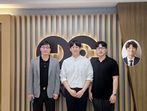
 Simultaneous Analysis of 21 Chemical Reactions... AI to Transform New Drug Development
< Photo 1. (From left) Professor Hyunwoo Kim and students Donghun Kim and Gyeongseon Choi in the Integrated M.S./Ph.D. program of the Department of Chemistry >
Thalidomide, a drug once used to alleviate morning sickness in pregnant women, exhibits distinct properties due to its optical isomers* in the body: one isomer has a sedative effect, while the other causes severe side effects like birth defects. As this example illustrates, precise organic synthesis techniques, which selectively synthesize only the desired optical isomer, are crucial in new drug development. Overcoming the traditional methods that struggled with simultaneously analyzing multiple reactants, our research team has developed the world's first technology to precisely analyze 21 types of reactants simultaneously. This breakthrough is expected to make a significant contribution to new drug development utilizing AI and robots.
*Optical Isomers: A pair of molecules with the same chemical formula that are mirror images of each other and cannot be superimposed due to their asymmetric structure. This is analogous to a left and right hand, which are similar in form but cannot be perfectly overlaid.
KAIST's Professor Hyunwoo Kim's research team in the Department of Chemistry announced on the 16th that they have developed an innovative optical isomer analysis technology suitable for the era of AI-driven autonomous synthesis*. This research is the world's first technology to precisely analyze asymmetric catalytic reactions involving multiple reactants simultaneously using high-resolution fluorine nuclear magnetic resonance spectroscopy (19F NMR). It is expected to make groundbreaking contributions to various fields, including new drug development and catalyst optimization.
*AI-driven Autonomous Synthesis: An advanced technology that automates and optimizes chemical substance synthesis processes using artificial intelligence (AI). It is gaining attention as a core element for realizing automated and intelligent research environments in future laboratories. AI predicts and adjusts experimental conditions, interprets results, and designs subsequent experiments independently, minimizing human intervention in repetitive experiments and significantly increasing research efficiency and innovativeness.
Currently, while autonomous synthesis systems can automate everything from reaction design to execution, reaction analysis still relies on individual processing using traditional equipment. This leads to slower speeds and bottlenecks, making it unsuitable for high-speed repetitive experiments.
Furthermore, multi-substrate simultaneous screening techniques proposed in the 1990s garnered attention as a strategy to maximize reaction analysis efficiency. However, limitations of existing chromatography-based analysis methods restricted the number of applicable substrates. In asymmetric synthesis reactions, which selectively synthesize only the desired optical isomer, simultaneously analyzing more than 10 types of substrates was nearly impossible.
< Figure 1. Conventional organic reaction evaluation methods follow a process of deriving optimal reaction conditions using a single substrate, then expanding the substrate scope one by one under those conditions, leaving potential reaction areas unexplored. To overcome this, high-throughput screening is introduced to broadly explore catalyst reactivity for various substrates. When combined with multi-substrate screening, this approach allows for a much broader and more systematic understanding of reaction scope and trends. >
To overcome these limitations, the research team developed a 19F NMR-based multi-substrate simultaneous screening technology. This method involves performing asymmetric catalytic reactions with multiple reactants in a single reaction vessel, introducing a fluorine functional group into the products, and then applying their self-developed chiral cobalt reagent to clearly quantify all optical isomers using 19F NMR.
Utilizing the excellent resolution and sensitivity of 19F NMR, the research team successfully performed asymmetric synthesis reactions of 21 substrates simultaneously in a single reaction vessel and quantitatively measured the product yield and optical isomer ratio without any separate purification steps.
Professor Hyunwoo Kim stated, "While anyone can perform asymmetric synthesis reactions with multiple substrates in one reactor, accurately analyzing all the products has been a challenging problem to solve until now. We expect that achieving world-class multi-substrate screening analysis technology will greatly contribute to enhancing the analytical capabilities of AI-driven autonomous synthesis platforms."
< Figure 2. A method for analyzing multi-substrate asymmetric catalytic reactions, where different substrates react simultaneously in a single reactor, using fluorine nuclear magnetic resonance has been implemented. By utilizing the characteristics of fluorine nuclear magnetic resonance, which has a clean background signal and a wide chemical shift range, the reactivity of each substrate can be quantitatively analyzed. It is also shown that the optical activity of all reactants can be simultaneously measured using a cobalt metal complex. >
He further added, "This research provides a technology that can rapidly verify the efficiency and selectivity of asymmetric catalytic reactions essential for new drug development, and it is expected to be utilized as a core analytical tool for AI-driven autonomous research."
< Figure 3. It can be seen that in a multi-substrate reductive amination reaction using a total of 21 substrates, the yield and optical activity of the reactants according to the catalyst system were simultaneously measured using a fluorine nuclear magnetic resonance-based analysis platform. The yield of each reactant is indicated by color saturation, and the optical activity by numbers. >
Donghun Kim (first author, Integrated M.S./Ph.D. program) and Gyeongseon Choi (second author, Integrated M.S./Ph.D. program) from the KAIST Department of Chemistry participated in this research. The study was published online in the Journal of the American Chemical Society on May 27, 2025.※ Paper Title: One-pot Multisubstrate Screening for Asymmetric Catalysis Enabled by 19F NMR-based Simultaneous Chiral Analysis※ DOI: 10.1021/jacs.5c03446
This research was supported by the National Research Foundation of Korea's Mid-Career Researcher Program, the Asymmetric Catalytic Reaction Design Center, and the KAIST KC30 Project.
< Figure 4. Conceptual diagram of performing multi-substrate screening reactions and utilizing fluorine nuclear magnetic resonance spectroscopy. >
2025.06.16 View 1139
Simultaneous Analysis of 21 Chemical Reactions... AI to Transform New Drug Development
< Photo 1. (From left) Professor Hyunwoo Kim and students Donghun Kim and Gyeongseon Choi in the Integrated M.S./Ph.D. program of the Department of Chemistry >
Thalidomide, a drug once used to alleviate morning sickness in pregnant women, exhibits distinct properties due to its optical isomers* in the body: one isomer has a sedative effect, while the other causes severe side effects like birth defects. As this example illustrates, precise organic synthesis techniques, which selectively synthesize only the desired optical isomer, are crucial in new drug development. Overcoming the traditional methods that struggled with simultaneously analyzing multiple reactants, our research team has developed the world's first technology to precisely analyze 21 types of reactants simultaneously. This breakthrough is expected to make a significant contribution to new drug development utilizing AI and robots.
*Optical Isomers: A pair of molecules with the same chemical formula that are mirror images of each other and cannot be superimposed due to their asymmetric structure. This is analogous to a left and right hand, which are similar in form but cannot be perfectly overlaid.
KAIST's Professor Hyunwoo Kim's research team in the Department of Chemistry announced on the 16th that they have developed an innovative optical isomer analysis technology suitable for the era of AI-driven autonomous synthesis*. This research is the world's first technology to precisely analyze asymmetric catalytic reactions involving multiple reactants simultaneously using high-resolution fluorine nuclear magnetic resonance spectroscopy (19F NMR). It is expected to make groundbreaking contributions to various fields, including new drug development and catalyst optimization.
*AI-driven Autonomous Synthesis: An advanced technology that automates and optimizes chemical substance synthesis processes using artificial intelligence (AI). It is gaining attention as a core element for realizing automated and intelligent research environments in future laboratories. AI predicts and adjusts experimental conditions, interprets results, and designs subsequent experiments independently, minimizing human intervention in repetitive experiments and significantly increasing research efficiency and innovativeness.
Currently, while autonomous synthesis systems can automate everything from reaction design to execution, reaction analysis still relies on individual processing using traditional equipment. This leads to slower speeds and bottlenecks, making it unsuitable for high-speed repetitive experiments.
Furthermore, multi-substrate simultaneous screening techniques proposed in the 1990s garnered attention as a strategy to maximize reaction analysis efficiency. However, limitations of existing chromatography-based analysis methods restricted the number of applicable substrates. In asymmetric synthesis reactions, which selectively synthesize only the desired optical isomer, simultaneously analyzing more than 10 types of substrates was nearly impossible.
< Figure 1. Conventional organic reaction evaluation methods follow a process of deriving optimal reaction conditions using a single substrate, then expanding the substrate scope one by one under those conditions, leaving potential reaction areas unexplored. To overcome this, high-throughput screening is introduced to broadly explore catalyst reactivity for various substrates. When combined with multi-substrate screening, this approach allows for a much broader and more systematic understanding of reaction scope and trends. >
To overcome these limitations, the research team developed a 19F NMR-based multi-substrate simultaneous screening technology. This method involves performing asymmetric catalytic reactions with multiple reactants in a single reaction vessel, introducing a fluorine functional group into the products, and then applying their self-developed chiral cobalt reagent to clearly quantify all optical isomers using 19F NMR.
Utilizing the excellent resolution and sensitivity of 19F NMR, the research team successfully performed asymmetric synthesis reactions of 21 substrates simultaneously in a single reaction vessel and quantitatively measured the product yield and optical isomer ratio without any separate purification steps.
Professor Hyunwoo Kim stated, "While anyone can perform asymmetric synthesis reactions with multiple substrates in one reactor, accurately analyzing all the products has been a challenging problem to solve until now. We expect that achieving world-class multi-substrate screening analysis technology will greatly contribute to enhancing the analytical capabilities of AI-driven autonomous synthesis platforms."
< Figure 2. A method for analyzing multi-substrate asymmetric catalytic reactions, where different substrates react simultaneously in a single reactor, using fluorine nuclear magnetic resonance has been implemented. By utilizing the characteristics of fluorine nuclear magnetic resonance, which has a clean background signal and a wide chemical shift range, the reactivity of each substrate can be quantitatively analyzed. It is also shown that the optical activity of all reactants can be simultaneously measured using a cobalt metal complex. >
He further added, "This research provides a technology that can rapidly verify the efficiency and selectivity of asymmetric catalytic reactions essential for new drug development, and it is expected to be utilized as a core analytical tool for AI-driven autonomous research."
< Figure 3. It can be seen that in a multi-substrate reductive amination reaction using a total of 21 substrates, the yield and optical activity of the reactants according to the catalyst system were simultaneously measured using a fluorine nuclear magnetic resonance-based analysis platform. The yield of each reactant is indicated by color saturation, and the optical activity by numbers. >
Donghun Kim (first author, Integrated M.S./Ph.D. program) and Gyeongseon Choi (second author, Integrated M.S./Ph.D. program) from the KAIST Department of Chemistry participated in this research. The study was published online in the Journal of the American Chemical Society on May 27, 2025.※ Paper Title: One-pot Multisubstrate Screening for Asymmetric Catalysis Enabled by 19F NMR-based Simultaneous Chiral Analysis※ DOI: 10.1021/jacs.5c03446
This research was supported by the National Research Foundation of Korea's Mid-Career Researcher Program, the Asymmetric Catalytic Reaction Design Center, and the KAIST KC30 Project.
< Figure 4. Conceptual diagram of performing multi-substrate screening reactions and utilizing fluorine nuclear magnetic resonance spectroscopy. >
2025.06.16 View 1139 -
 “One Experiment Is All It Takes”: KAIST Team Revolutionizes Drug Interaction Testing, Replacing 60,000 Studies
A groundbreaking new method developed by researchers at KAIST and Chungnam National University could drastically streamline drug interaction testing — replacing dozens of traditional experiments with just one.
The research, led by Professor Jae Kyoung Kim of KAIST Department of Mathematical Sciences & IBS Biomedical Mathematics Group and Professor Sang Kyum Kim of Chungnam National University's College of Pharmacy, introduces a novel analysis technique called 50-BOA, published in Nature Communications on June 5, 2025.
< Photo 1. (From left) Professor Sang Kyum Kim (Chungnam National University College of Pharmacy, co-corresponding author), Dr. Yun Min Song (IBS Biomedical Mathematics Group, formerly KAIST Department of Mathematical Sciences, co-first author), undergraduate student Hyeong Jun Jang (KAIST, co-first author), Professor Jae Kyoung Kim (KAIST and IBS Biomedical Mathematics Group, co-corresponding author) (Top left in the bubble) Professor Hwi-yeol Yun (Chungnam National University College of Pharmacy, co-author) >
For decades, scientists have had to repeat drug inhibition experiments across a wide range of concentrations to estimate inhibition constants — a process seen in over 60,000 scientific publications. But the KAIST-led team discovered that a single, well-chosen inhibitor concentration can yield even more accurate results.
< Figure 1. Graphical summary of 50-BOA. 50-BOA improves the accuracy and efficiency of inhibition constant estimation by using only a single inhibitor concentration instead of the traditionally used method of employing multiple inhibitor concentrations. >
“This approach challenges long-standing assumptions in experimental pharmacology,” says Prof. Kim. “It shows how mathematics can fundamentally redesign life science experiments.”
By mathematically analyzing the sources of error in conventional methods, the team found that over half the data typically collected adds no value or even skews results. Their new method not only cuts experimental effort by over 75%, but also enhances reproducibility and accuracy.
To help researchers adopt the method quickly, the team developed a user-friendly tool that takes simple Excel files as input, now freely available on GitHub:
☞ https://github.com/Mathbiomed/50-BOA
< Figure 2. The MATLAB and R package of 50-BOA at GitHub >
The work holds promise for faster and more reliable drug development, especially in assessing potential interactions in combination therapies. The U.S. FDA already emphasizes the importance of accurate enzyme inhibition assessment during early-stage drug evaluation — and this method could soon become a new gold standard.
2025.06.16 View 1315
“One Experiment Is All It Takes”: KAIST Team Revolutionizes Drug Interaction Testing, Replacing 60,000 Studies
A groundbreaking new method developed by researchers at KAIST and Chungnam National University could drastically streamline drug interaction testing — replacing dozens of traditional experiments with just one.
The research, led by Professor Jae Kyoung Kim of KAIST Department of Mathematical Sciences & IBS Biomedical Mathematics Group and Professor Sang Kyum Kim of Chungnam National University's College of Pharmacy, introduces a novel analysis technique called 50-BOA, published in Nature Communications on June 5, 2025.
< Photo 1. (From left) Professor Sang Kyum Kim (Chungnam National University College of Pharmacy, co-corresponding author), Dr. Yun Min Song (IBS Biomedical Mathematics Group, formerly KAIST Department of Mathematical Sciences, co-first author), undergraduate student Hyeong Jun Jang (KAIST, co-first author), Professor Jae Kyoung Kim (KAIST and IBS Biomedical Mathematics Group, co-corresponding author) (Top left in the bubble) Professor Hwi-yeol Yun (Chungnam National University College of Pharmacy, co-author) >
For decades, scientists have had to repeat drug inhibition experiments across a wide range of concentrations to estimate inhibition constants — a process seen in over 60,000 scientific publications. But the KAIST-led team discovered that a single, well-chosen inhibitor concentration can yield even more accurate results.
< Figure 1. Graphical summary of 50-BOA. 50-BOA improves the accuracy and efficiency of inhibition constant estimation by using only a single inhibitor concentration instead of the traditionally used method of employing multiple inhibitor concentrations. >
“This approach challenges long-standing assumptions in experimental pharmacology,” says Prof. Kim. “It shows how mathematics can fundamentally redesign life science experiments.”
By mathematically analyzing the sources of error in conventional methods, the team found that over half the data typically collected adds no value or even skews results. Their new method not only cuts experimental effort by over 75%, but also enhances reproducibility and accuracy.
To help researchers adopt the method quickly, the team developed a user-friendly tool that takes simple Excel files as input, now freely available on GitHub:
☞ https://github.com/Mathbiomed/50-BOA
< Figure 2. The MATLAB and R package of 50-BOA at GitHub >
The work holds promise for faster and more reliable drug development, especially in assessing potential interactions in combination therapies. The U.S. FDA already emphasizes the importance of accurate enzyme inhibition assessment during early-stage drug evaluation — and this method could soon become a new gold standard.
2025.06.16 View 1315 -
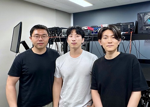 High-Resolution Spectrometer that Fits into Smartphones Developed by KAIST Researchers
- Professor Mooseok Jang's research team at the Department of Bio and Brain Engineering develops an ultra-compact, high-resolution spectrometer using 'double-layer disordered metasurfaces' that generate unique random patterns depending on light's color.
- Unlike conventional dispersion-based spectrometers that were difficult to apply to portable devices, this new concept spectrometer technology achieves 1nm-level high resolution in a device smaller than 1cm, comparable in size to a fingernail.
- It can be utilized as a built-in spectrometer in smartphones and wearable devices in the future, and can be expanded to advanced optical technologies such as hyperspectral imaging and ultrafast imaging.
< Photo 1. (From left) Professor Mooseok Jang, Dong-gu Lee (Ph.D. candidate), Gookho Song (Ph.D. candidate) >
Color, as the way light's wavelength is perceived by the human eye, goes beyond a simple aesthetic element, containing important scientific information like a substance's composition or state. Spectrometers are optical devices that analyze material properties by decomposing light into its constituent wavelengths, and they are widely used in various scientific and industrial fields, including material analysis, chemical component detection, and life science research. Existing high-resolution spectrometers were large and complex, making them difficult for widespread daily use. However, thanks to the ultra-compact, high-resolution spectrometer developed by KAIST researchers, it is now expected that light's color information can be utilized even within smartphones or wearable devices.
KAIST (President Kwang Hyung Lee) announced on the 13th that Professor Mooseok Jang's research team at the Department of Bio and Brain Engineering has successfully developed a reconstruction-based spectrometer technology using double-layer disordered metasurfaces*.
*Double-layer disordered metasurface: An innovative optical device that complexly scatters light through two layers of disordered nanostructures, creating unique and predictable speckle patterns for each wavelength.
Existing high-resolution spectrometers have a large form factor, on the order of tens of centimeters, and require complex calibration processes to maintain accuracy. This fundamentally stems from the operating principle of traditional dispersive elements, such as gratings and prisms, which separate light wavelengths along the propagation direction, much like a rainbow separates colors. Consequently, despite the potential for light's color information to be widely useful in daily life, spectroscopic technology has been limited to laboratory or industrial manufacturing environments.
< Figure 1. Through a simple structure consisting of a double layer of disordered metasurfaces and an image sensor, it was shown that speckles of predictable spectral channels with high spectral resolution can be generated in a compact form factor. The high similarity between the measured and calculated speckles was used to solve the inverse problem and verify the ability to reconstruct the spectrum. >
The research team devised a method that departs from the conventional spectroscopic paradigm of using diffraction gratings or prisms, which establish a one-to-one correspondence between light's color information and its propagation direction, by utilizing designed disordered structures as optical components. In this process, they employed metasurfaces, which can freely control the light propagation process using structures tens to hundreds of nanometers in size, to accurately implement 'complex random patterns (speckle*)'.
*Speckle: An irregular pattern of light intensity created by the interference of multiple wavefronts of light.
Specifically, they developed a method that involves implementing a double-layer disordered metasurface to generate wavelength-specific speckle patterns and then reconstructing precise color information (wavelength) of the light from the random patterns measured by a camera.
As a result, they successfully developed a new concept spectrometer technology that can accurately measure light across a broad range of visible to infrared (440-1,300nm) with a high resolution of 1 nanometer (nm) in a device smaller than a fingernail (less than 1cm) using only a single image capture.
< Figure 2. A disordered metasurface is a metasurface with irregularly arranged structures ranging from tens to hundreds of nanometers in size. In a double-layer structure, a propagation space is placed between the two metasurfaces to control the output speckle with high degrees of freedom, thereby achieving a spectral resolution of 1 nm even in a form factor smaller than 1 cm. >
Dong-gu Lee, a lead author of this study, stated, "This technology is implemented in a way that is directly integrated with commercial image sensors, and we expect that it will enable easy acquisition and utilization of light's wavelength information in daily life when built into mobile devices in the future."
Professor Mooseok Jang said, "This technology overcomes the limitations of existing RGB three-color based machine vision fields, which only distinguish and recognize three color components (red, green, blue), and has diverse applications. We anticipate various applied research for this technology, which expands the horizon of laboratory-level technology to daily-level machine vision technology for applications such as food component analysis, crop health diagnosis, skin health measurement, environmental pollution detection, and bio/medical diagnostics." He added, "Furthermore, it can be extended to various advanced optical technologies such as hyperspectral imaging, which records wavelength and spatial information simultaneously with high resolution, 3D optical trapping technology, which precisely controls light of multiple wavelengths into desired forms, and ultrafast imaging technology, which captures phenomena occurring in very short periods."
This research was collaboratively led by Dong-gu Lee (Ph.D. candidate) and Gookho Song (Ph.D. candidate) from the KAIST Department of Bio and Brain Engineering as co-first authors, with Professor Mooseok Jang as the corresponding author. The findings were published online in the international journal Science Advances on May 28, 2025.* Paper Title: Reconstructive spectrometer using double-layer disordered metasurfaces* DOI: 10.1126/sciadv.adv2376
This research was supported by the Samsung Research Funding and Incubation Center of Samsung Electronics grant, the National Research Foundation of Korea (NRF) grant funded by the Korea government (MSIT), and the Bio & Medical Technology Development Program of the National Research Foundation (NRF) funded by the Korean government (MSIT).
2025.06.13 View 1186
High-Resolution Spectrometer that Fits into Smartphones Developed by KAIST Researchers
- Professor Mooseok Jang's research team at the Department of Bio and Brain Engineering develops an ultra-compact, high-resolution spectrometer using 'double-layer disordered metasurfaces' that generate unique random patterns depending on light's color.
- Unlike conventional dispersion-based spectrometers that were difficult to apply to portable devices, this new concept spectrometer technology achieves 1nm-level high resolution in a device smaller than 1cm, comparable in size to a fingernail.
- It can be utilized as a built-in spectrometer in smartphones and wearable devices in the future, and can be expanded to advanced optical technologies such as hyperspectral imaging and ultrafast imaging.
< Photo 1. (From left) Professor Mooseok Jang, Dong-gu Lee (Ph.D. candidate), Gookho Song (Ph.D. candidate) >
Color, as the way light's wavelength is perceived by the human eye, goes beyond a simple aesthetic element, containing important scientific information like a substance's composition or state. Spectrometers are optical devices that analyze material properties by decomposing light into its constituent wavelengths, and they are widely used in various scientific and industrial fields, including material analysis, chemical component detection, and life science research. Existing high-resolution spectrometers were large and complex, making them difficult for widespread daily use. However, thanks to the ultra-compact, high-resolution spectrometer developed by KAIST researchers, it is now expected that light's color information can be utilized even within smartphones or wearable devices.
KAIST (President Kwang Hyung Lee) announced on the 13th that Professor Mooseok Jang's research team at the Department of Bio and Brain Engineering has successfully developed a reconstruction-based spectrometer technology using double-layer disordered metasurfaces*.
*Double-layer disordered metasurface: An innovative optical device that complexly scatters light through two layers of disordered nanostructures, creating unique and predictable speckle patterns for each wavelength.
Existing high-resolution spectrometers have a large form factor, on the order of tens of centimeters, and require complex calibration processes to maintain accuracy. This fundamentally stems from the operating principle of traditional dispersive elements, such as gratings and prisms, which separate light wavelengths along the propagation direction, much like a rainbow separates colors. Consequently, despite the potential for light's color information to be widely useful in daily life, spectroscopic technology has been limited to laboratory or industrial manufacturing environments.
< Figure 1. Through a simple structure consisting of a double layer of disordered metasurfaces and an image sensor, it was shown that speckles of predictable spectral channels with high spectral resolution can be generated in a compact form factor. The high similarity between the measured and calculated speckles was used to solve the inverse problem and verify the ability to reconstruct the spectrum. >
The research team devised a method that departs from the conventional spectroscopic paradigm of using diffraction gratings or prisms, which establish a one-to-one correspondence between light's color information and its propagation direction, by utilizing designed disordered structures as optical components. In this process, they employed metasurfaces, which can freely control the light propagation process using structures tens to hundreds of nanometers in size, to accurately implement 'complex random patterns (speckle*)'.
*Speckle: An irregular pattern of light intensity created by the interference of multiple wavefronts of light.
Specifically, they developed a method that involves implementing a double-layer disordered metasurface to generate wavelength-specific speckle patterns and then reconstructing precise color information (wavelength) of the light from the random patterns measured by a camera.
As a result, they successfully developed a new concept spectrometer technology that can accurately measure light across a broad range of visible to infrared (440-1,300nm) with a high resolution of 1 nanometer (nm) in a device smaller than a fingernail (less than 1cm) using only a single image capture.
< Figure 2. A disordered metasurface is a metasurface with irregularly arranged structures ranging from tens to hundreds of nanometers in size. In a double-layer structure, a propagation space is placed between the two metasurfaces to control the output speckle with high degrees of freedom, thereby achieving a spectral resolution of 1 nm even in a form factor smaller than 1 cm. >
Dong-gu Lee, a lead author of this study, stated, "This technology is implemented in a way that is directly integrated with commercial image sensors, and we expect that it will enable easy acquisition and utilization of light's wavelength information in daily life when built into mobile devices in the future."
Professor Mooseok Jang said, "This technology overcomes the limitations of existing RGB three-color based machine vision fields, which only distinguish and recognize three color components (red, green, blue), and has diverse applications. We anticipate various applied research for this technology, which expands the horizon of laboratory-level technology to daily-level machine vision technology for applications such as food component analysis, crop health diagnosis, skin health measurement, environmental pollution detection, and bio/medical diagnostics." He added, "Furthermore, it can be extended to various advanced optical technologies such as hyperspectral imaging, which records wavelength and spatial information simultaneously with high resolution, 3D optical trapping technology, which precisely controls light of multiple wavelengths into desired forms, and ultrafast imaging technology, which captures phenomena occurring in very short periods."
This research was collaboratively led by Dong-gu Lee (Ph.D. candidate) and Gookho Song (Ph.D. candidate) from the KAIST Department of Bio and Brain Engineering as co-first authors, with Professor Mooseok Jang as the corresponding author. The findings were published online in the international journal Science Advances on May 28, 2025.* Paper Title: Reconstructive spectrometer using double-layer disordered metasurfaces* DOI: 10.1126/sciadv.adv2376
This research was supported by the Samsung Research Funding and Incubation Center of Samsung Electronics grant, the National Research Foundation of Korea (NRF) grant funded by the Korea government (MSIT), and the Bio & Medical Technology Development Program of the National Research Foundation (NRF) funded by the Korean government (MSIT).
2025.06.13 View 1186 -
 KAIST Predicts Diseases by Early Detection of Aging Signals in Liver Tissue
- KAIST-KRIBB Develops ‘FiNi-seq’ Technology to Capture Characteristics of Fibrotic Microenvironments Accumulated in Liver Tissue and Dynamic Changes of Early Aging Cells
- Elucidation of the Spatial Ecosystem of Aged Liver Tissue, where Reprogramming of Senescent Cells and Immune Exhaustion Progresses, at the Single-Cell Genome and Epigenome Levels
< (From left) Professor Jong-Eun Park of KAIST Graduate School of Medical Science and Engineering (GSMSE), Dr. Chuna Kim of KRIBB, Dr. Kwon Yong Tak of KAIST GSMSE, Ph.D. Candidate Juyeon Kim of KRIBB, Ph.D. Candidate Myungsun Park of KAIST GSMSE >
Aging and chronic diseases involve the gradual accumulation of subtle tissue changes over a long period. Therefore, there are still limitations in quantitatively understanding these changes within organs and linking them to early signs of disease onset. In response, Korean researchers have successfully developed a platform technology that accurately captures localized changes that first occur within tissue, significantly aiding in faster disease discovery and prediction, and in setting personalized treatment targets.
KAIST (President Kwang Hyung Lee) announced on June 12th that a joint research team led by Professor Jong-Eun Park of the Graduate School of Medical Science and Engineering at KAIST and Dr. Chuna Kim of the Aging Convergence Research Center at the Korea Research Institute of Bioscience and Biotechnology (KRIBB, President Seok-Yoon Kwon) has developed ‘FiNi-seq (Fibrotic Niche enrichment sequencing)’ technology. This technology captures fibrotic microenvironments locally occurring in aged liver tissue and enables precise analysis at the single-cell transcriptome level*.
*Single-cell transcriptome analysis: A method to measure how actively each cell uses which genes, allowing identification and function of individual diseased cells.
The researchers developed a method to selectively enrich early aging microenvironments where regeneration is delayed and fibrosis accumulates, by physically selecting regions with high tissue degradation resistance in aged liver tissue.
In this process, high-resolution identification of fibrosis-related endothelial cells, fibroblasts interacting with the immune system, and immune-exhausted cells such as PD-1 highly expressing CD8 T cells, which were difficult to capture with existing single-cell analysis technologies, was possible.
In particular, the research team confirmed through ‘FiNi-seq’ technology that specific cells observed in fibrotic areas within aged liver tissue secondarily age the surrounding environment through secreted factors, and that this leads to the expansion of the aged environment.
Furthermore, they also elucidated the mechanism by which endothelial cells lose their tissue-specific identity and induce innate immune responses, promoting immune cell infiltration. Through spatial transcriptome analysis, the spatial distribution of fibroblasts interacting with immune cells was quantified, revealing their involvement in tissue regeneration, induction of inflammatory responses, and progression to chronic fibrosis.
The research team performed integrated analysis of multi-omics\* data to obtain transcriptome and epigenome information, precisely interpreting the microenvironment of aged liver tissue and its spatial heterogeneity, and confirming how these changes are connected to the intrahepatic vascular structure.
*Multi-omics: An integrated analysis method for various biological information within an organism, such as genes, proteins, metabolites, and cell information.
The newly developed ‘FiNi-seq’ technology is expected to be a useful platform for high-resolution capture of pathophysiological signals in most chronic liver diseases, including the aging process that causes fibrosis.
< Figure 1. Isolation of fibrotic regions from aged liver tissue, followed by single-cell transcriptome analysis and validation in a fibrosis model. >
The first author, Dr. Kwon Yong Tak of KAIST Graduate School of Medical Science and Engineering (GSMSE), a hepatologist at Seoul St. Mary's Hospital, designed this study to lay the groundwork for early diagnosis and treatment of fibrosis progression, the most important clinical prognostic indicator in chronic liver disease, while pursuing his Ph.D. at KAIST KAIST GSMSE with support from the physician-scientist training program. Co-first author Myungsun Park, a Ph.D. candidate at KAIST KAIST GSMSE, was responsible for the technical implementation of FiNi-seq technology, and Juyeon Kim, a Ph.D. candidate at KRIBB's Aging Convergence Research Center, was responsible for imaging analysis of aged tissue, playing a key role in the research.
Dr. Chuna Kim of KRIBB stated, “Through this study, we were able to precisely elucidate the cellular composition and spatial characteristics of the fibrotic microenvironment observed in aged liver tissue at the single-cell level.”
< Figure 2. Spatially defined stepwise progression patterns of aging-related regions within the liver and identification of regulatory factors inducing them. >
Professor Jong-Eun Park of the Graduate School of Medical Science and Engineering said, “As an analytical technology that can capture subtle changes occurring in the early stages of aging and chronic diseases, it is expected to play a significant role in finding effective treatment targets in the future. Also, we plan to expand this research to chronic diseases in other organs such as the lungs and kidneys, as well as various liver disease models.”
This research was published in the international journal ‘Nature Aging’ on May 5, 2025, with Dr. Kwon Yong Tak of KAIST KAIST GSMSE, Ph.D. Candidate Juyeon Kim of KRIBB, and Ph.D. Candidate Myungsun Park of KAIST as co-first authors.
*Paper Title: Quasi-spatial single-cell transcriptome based on physical tissue properties defines early aging associated niche in liver
*DOI: https://doi.org/10.1038/s43587-025-00857-7
This research was supported by several domestic institutions, including the National Research Foundation of Korea, the Korea Health Industry Development Institute (KHIDI), the Korea Research Institute of Bioscience and Biotechnology (KRIBB), KIST, POSCO Science Fellowship, and the Convergence Medical Scientist Training Program.
2025.06.12 View 1053
KAIST Predicts Diseases by Early Detection of Aging Signals in Liver Tissue
- KAIST-KRIBB Develops ‘FiNi-seq’ Technology to Capture Characteristics of Fibrotic Microenvironments Accumulated in Liver Tissue and Dynamic Changes of Early Aging Cells
- Elucidation of the Spatial Ecosystem of Aged Liver Tissue, where Reprogramming of Senescent Cells and Immune Exhaustion Progresses, at the Single-Cell Genome and Epigenome Levels
< (From left) Professor Jong-Eun Park of KAIST Graduate School of Medical Science and Engineering (GSMSE), Dr. Chuna Kim of KRIBB, Dr. Kwon Yong Tak of KAIST GSMSE, Ph.D. Candidate Juyeon Kim of KRIBB, Ph.D. Candidate Myungsun Park of KAIST GSMSE >
Aging and chronic diseases involve the gradual accumulation of subtle tissue changes over a long period. Therefore, there are still limitations in quantitatively understanding these changes within organs and linking them to early signs of disease onset. In response, Korean researchers have successfully developed a platform technology that accurately captures localized changes that first occur within tissue, significantly aiding in faster disease discovery and prediction, and in setting personalized treatment targets.
KAIST (President Kwang Hyung Lee) announced on June 12th that a joint research team led by Professor Jong-Eun Park of the Graduate School of Medical Science and Engineering at KAIST and Dr. Chuna Kim of the Aging Convergence Research Center at the Korea Research Institute of Bioscience and Biotechnology (KRIBB, President Seok-Yoon Kwon) has developed ‘FiNi-seq (Fibrotic Niche enrichment sequencing)’ technology. This technology captures fibrotic microenvironments locally occurring in aged liver tissue and enables precise analysis at the single-cell transcriptome level*.
*Single-cell transcriptome analysis: A method to measure how actively each cell uses which genes, allowing identification and function of individual diseased cells.
The researchers developed a method to selectively enrich early aging microenvironments where regeneration is delayed and fibrosis accumulates, by physically selecting regions with high tissue degradation resistance in aged liver tissue.
In this process, high-resolution identification of fibrosis-related endothelial cells, fibroblasts interacting with the immune system, and immune-exhausted cells such as PD-1 highly expressing CD8 T cells, which were difficult to capture with existing single-cell analysis technologies, was possible.
In particular, the research team confirmed through ‘FiNi-seq’ technology that specific cells observed in fibrotic areas within aged liver tissue secondarily age the surrounding environment through secreted factors, and that this leads to the expansion of the aged environment.
Furthermore, they also elucidated the mechanism by which endothelial cells lose their tissue-specific identity and induce innate immune responses, promoting immune cell infiltration. Through spatial transcriptome analysis, the spatial distribution of fibroblasts interacting with immune cells was quantified, revealing their involvement in tissue regeneration, induction of inflammatory responses, and progression to chronic fibrosis.
The research team performed integrated analysis of multi-omics\* data to obtain transcriptome and epigenome information, precisely interpreting the microenvironment of aged liver tissue and its spatial heterogeneity, and confirming how these changes are connected to the intrahepatic vascular structure.
*Multi-omics: An integrated analysis method for various biological information within an organism, such as genes, proteins, metabolites, and cell information.
The newly developed ‘FiNi-seq’ technology is expected to be a useful platform for high-resolution capture of pathophysiological signals in most chronic liver diseases, including the aging process that causes fibrosis.
< Figure 1. Isolation of fibrotic regions from aged liver tissue, followed by single-cell transcriptome analysis and validation in a fibrosis model. >
The first author, Dr. Kwon Yong Tak of KAIST Graduate School of Medical Science and Engineering (GSMSE), a hepatologist at Seoul St. Mary's Hospital, designed this study to lay the groundwork for early diagnosis and treatment of fibrosis progression, the most important clinical prognostic indicator in chronic liver disease, while pursuing his Ph.D. at KAIST KAIST GSMSE with support from the physician-scientist training program. Co-first author Myungsun Park, a Ph.D. candidate at KAIST KAIST GSMSE, was responsible for the technical implementation of FiNi-seq technology, and Juyeon Kim, a Ph.D. candidate at KRIBB's Aging Convergence Research Center, was responsible for imaging analysis of aged tissue, playing a key role in the research.
Dr. Chuna Kim of KRIBB stated, “Through this study, we were able to precisely elucidate the cellular composition and spatial characteristics of the fibrotic microenvironment observed in aged liver tissue at the single-cell level.”
< Figure 2. Spatially defined stepwise progression patterns of aging-related regions within the liver and identification of regulatory factors inducing them. >
Professor Jong-Eun Park of the Graduate School of Medical Science and Engineering said, “As an analytical technology that can capture subtle changes occurring in the early stages of aging and chronic diseases, it is expected to play a significant role in finding effective treatment targets in the future. Also, we plan to expand this research to chronic diseases in other organs such as the lungs and kidneys, as well as various liver disease models.”
This research was published in the international journal ‘Nature Aging’ on May 5, 2025, with Dr. Kwon Yong Tak of KAIST KAIST GSMSE, Ph.D. Candidate Juyeon Kim of KRIBB, and Ph.D. Candidate Myungsun Park of KAIST as co-first authors.
*Paper Title: Quasi-spatial single-cell transcriptome based on physical tissue properties defines early aging associated niche in liver
*DOI: https://doi.org/10.1038/s43587-025-00857-7
This research was supported by several domestic institutions, including the National Research Foundation of Korea, the Korea Health Industry Development Institute (KHIDI), the Korea Research Institute of Bioscience and Biotechnology (KRIBB), KIST, POSCO Science Fellowship, and the Convergence Medical Scientist Training Program.
2025.06.12 View 1053 -
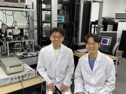 KAIST Turns an Unprecedented Idea into Reality: Quantum Computing with Magnets
What started as an idea under KAIST’s Global Singularity Research Project—"Can we build a quantum computer using magnets?"—has now become a scientific reality. A KAIST-led international research team has successfully demonstrated a core quantum computing technology using magnetic materials (ferromagnets) for the first time in the world.
KAIST (represented by President Kwang-Hyung Lee) announced on the 6th of May that a team led by Professor Kab-Jin Kim from the Department of Physics, in collaboration with the Argonne National Laboratory and the University of Illinois Urbana-Champaign (UIUC), has developed a “photon-magnon hybrid chip” and successfully implemented real-time, multi-pulse interference using magnetic materials—marking a global first.
< Photo 1. Dr. Moojune Song (left) and Professor Kab-Jin Kim (right) of KAIST Department of Physics >
In simple terms, the researchers developed a special chip that synchronizes light and internal magnetic vibrations (magnons), enabling the transmission of phase information between distant magnets. They succeeded in observing and controlling interference between multiple signals in real time. This marks the first experimental evidence that magnets can serve as key components in quantum computing, serving as a pivotal step toward magnet-based quantum platforms.
The N and S poles of a magnet stem from the spin of electrons inside atoms. When many atoms align, their collective spin vibrations create a quantum particle known as a “magnon.”
Magnons are especially promising because of their nonreciprocal nature—they can carry information in only one direction, which makes them suitable for quantum noise isolation in compact quantum chips. They can also couple with both light and microwaves, enabling the potential for long-distance quantum communication over tens of kilometers.
Moreover, using special materials like antiferromagnets could allow quantum computers to operate at terahertz (THz) frequencies, far surpassing today’s hardware limitations, and possibly enabling room-temperature quantum computing without the need for bulky cryogenic equipment.
To build such a system, however, one must be able to transmit, measure, and control the phase information of magnons—the starting point and propagation of their waveforms—in real time. This had not been achieved until now.
< Figure 1. Superconducting Circuit-Based Magnon-Photon Hybrid System. (a) Schematic diagram of the device. A NbN superconducting resonator circuit fabricated on a silicon substrate is coupled with spherical YIG magnets (250 μm diameter), and magnons are generated and measured in real-time via a vertical antenna. (b) Photograph of the actual device. The distance between the two YIG spheres is 12 mm, a distance at which they cannot influence each other without the superconducting circuit. >
Professor Kim’s team used two tiny magnetic spheres made of Yttrium Iron Garnet (YIG) placed 12 mm apart with a superconducting resonator in between—similar to those used in quantum processors by Google and IBM. They input pulses into one magnet and successfully observed lossless transmission of magnon vibrations to the second magnet via the superconducting circuit.
They confirmed that from single nanosecond pulses to four microwave pulses, the magnon vibrations maintained their phase information and demonstrated predictable constructive or destructive interference in real time—known as coherent interference.
By adjusting the pulse frequencies and their intervals, the researchers could also freely control the interference patterns of magnons, effectively showing for the first time that electrical signals can be used to manipulate magnonic quantum states.
This work demonstrated that quantum gate operations using multiple pulses—a fundamental technique in quantum information processing—can be implemented using a hybrid system of magnetic materials and superconducting circuits. This opens the door for the practical use of magnet-based quantum devices.
< Figure 2. Experimental Data. (a) Measurement results of magnon-magnon band anticrossing via continuous wave measurement, showing the formation of a strong coupling hybrid system. (b) Magnon pulse exchange oscillation phenomenon between YIG spheres upon single pulse application. It can be seen that magnon information is coherently transmitted at regular time intervals through the superconducting circuit. (c,d) Magnon interference phenomenon upon dual pulse application. The magnon information state can be arbitrarily controlled by adjusting the time interval and carrier frequency between pulses. >
Professor Kab-Jin Kim stated, “This project began with a bold, even unconventional idea proposed to the Global Singularity Research Program: ‘What if we could build a quantum computer with magnets?’ The journey has been fascinating, and this study not only opens a new field of quantum spintronics, but also marks a turning point in developing high-efficiency quantum information processing devices.”
The research was co-led by postdoctoral researcher Moojune Song (KAIST), Dr. Yi Li and Dr. Valentine Novosad from Argonne National Lab, and Prof. Axel Hoffmann’s team at UIUC. The results were published in Nature Communications on April 17 and npj Spintronics on April 1, 2025.
Paper 1: Single-shot magnon interference in a magnon-superconducting-resonator hybrid circuit, Nat. Commun. 16, 3649 (2025)
DOI: https://doi.org/10.1038/s41467-025-58482-2
Paper 2: Single-shot electrical detection of short-wavelength magnon pulse transmission in a magnonic ultra-thin-film waveguide, npj Spintronics 3, 12 (2025)
DOI: https://doi.org/10.1038/s44306-025-00072-5
The research was supported by KAIST’s Global Singularity Research Initiative, the National Research Foundation of Korea (including the Mid-Career Researcher, Leading Research Center, and Quantum Information Science Human Resource Development programs), and the U.S. Department of Energy.
2025.06.12 View 1998
KAIST Turns an Unprecedented Idea into Reality: Quantum Computing with Magnets
What started as an idea under KAIST’s Global Singularity Research Project—"Can we build a quantum computer using magnets?"—has now become a scientific reality. A KAIST-led international research team has successfully demonstrated a core quantum computing technology using magnetic materials (ferromagnets) for the first time in the world.
KAIST (represented by President Kwang-Hyung Lee) announced on the 6th of May that a team led by Professor Kab-Jin Kim from the Department of Physics, in collaboration with the Argonne National Laboratory and the University of Illinois Urbana-Champaign (UIUC), has developed a “photon-magnon hybrid chip” and successfully implemented real-time, multi-pulse interference using magnetic materials—marking a global first.
< Photo 1. Dr. Moojune Song (left) and Professor Kab-Jin Kim (right) of KAIST Department of Physics >
In simple terms, the researchers developed a special chip that synchronizes light and internal magnetic vibrations (magnons), enabling the transmission of phase information between distant magnets. They succeeded in observing and controlling interference between multiple signals in real time. This marks the first experimental evidence that magnets can serve as key components in quantum computing, serving as a pivotal step toward magnet-based quantum platforms.
The N and S poles of a magnet stem from the spin of electrons inside atoms. When many atoms align, their collective spin vibrations create a quantum particle known as a “magnon.”
Magnons are especially promising because of their nonreciprocal nature—they can carry information in only one direction, which makes them suitable for quantum noise isolation in compact quantum chips. They can also couple with both light and microwaves, enabling the potential for long-distance quantum communication over tens of kilometers.
Moreover, using special materials like antiferromagnets could allow quantum computers to operate at terahertz (THz) frequencies, far surpassing today’s hardware limitations, and possibly enabling room-temperature quantum computing without the need for bulky cryogenic equipment.
To build such a system, however, one must be able to transmit, measure, and control the phase information of magnons—the starting point and propagation of their waveforms—in real time. This had not been achieved until now.
< Figure 1. Superconducting Circuit-Based Magnon-Photon Hybrid System. (a) Schematic diagram of the device. A NbN superconducting resonator circuit fabricated on a silicon substrate is coupled with spherical YIG magnets (250 μm diameter), and magnons are generated and measured in real-time via a vertical antenna. (b) Photograph of the actual device. The distance between the two YIG spheres is 12 mm, a distance at which they cannot influence each other without the superconducting circuit. >
Professor Kim’s team used two tiny magnetic spheres made of Yttrium Iron Garnet (YIG) placed 12 mm apart with a superconducting resonator in between—similar to those used in quantum processors by Google and IBM. They input pulses into one magnet and successfully observed lossless transmission of magnon vibrations to the second magnet via the superconducting circuit.
They confirmed that from single nanosecond pulses to four microwave pulses, the magnon vibrations maintained their phase information and demonstrated predictable constructive or destructive interference in real time—known as coherent interference.
By adjusting the pulse frequencies and their intervals, the researchers could also freely control the interference patterns of magnons, effectively showing for the first time that electrical signals can be used to manipulate magnonic quantum states.
This work demonstrated that quantum gate operations using multiple pulses—a fundamental technique in quantum information processing—can be implemented using a hybrid system of magnetic materials and superconducting circuits. This opens the door for the practical use of magnet-based quantum devices.
< Figure 2. Experimental Data. (a) Measurement results of magnon-magnon band anticrossing via continuous wave measurement, showing the formation of a strong coupling hybrid system. (b) Magnon pulse exchange oscillation phenomenon between YIG spheres upon single pulse application. It can be seen that magnon information is coherently transmitted at regular time intervals through the superconducting circuit. (c,d) Magnon interference phenomenon upon dual pulse application. The magnon information state can be arbitrarily controlled by adjusting the time interval and carrier frequency between pulses. >
Professor Kab-Jin Kim stated, “This project began with a bold, even unconventional idea proposed to the Global Singularity Research Program: ‘What if we could build a quantum computer with magnets?’ The journey has been fascinating, and this study not only opens a new field of quantum spintronics, but also marks a turning point in developing high-efficiency quantum information processing devices.”
The research was co-led by postdoctoral researcher Moojune Song (KAIST), Dr. Yi Li and Dr. Valentine Novosad from Argonne National Lab, and Prof. Axel Hoffmann’s team at UIUC. The results were published in Nature Communications on April 17 and npj Spintronics on April 1, 2025.
Paper 1: Single-shot magnon interference in a magnon-superconducting-resonator hybrid circuit, Nat. Commun. 16, 3649 (2025)
DOI: https://doi.org/10.1038/s41467-025-58482-2
Paper 2: Single-shot electrical detection of short-wavelength magnon pulse transmission in a magnonic ultra-thin-film waveguide, npj Spintronics 3, 12 (2025)
DOI: https://doi.org/10.1038/s44306-025-00072-5
The research was supported by KAIST’s Global Singularity Research Initiative, the National Research Foundation of Korea (including the Mid-Career Researcher, Leading Research Center, and Quantum Information Science Human Resource Development programs), and the U.S. Department of Energy.
2025.06.12 View 1998