Keon+Jae+Lee
-
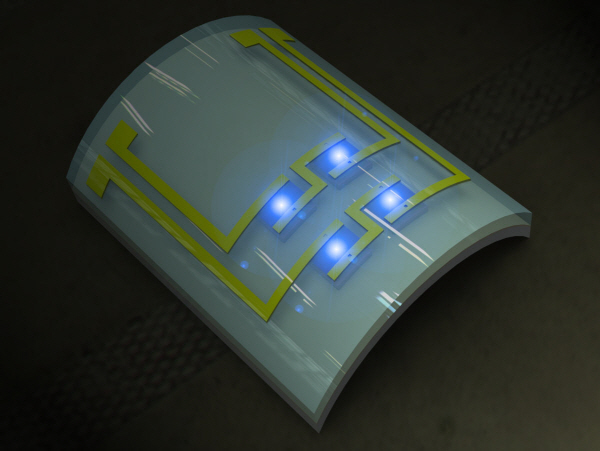
 Improving Silver Nanowires for FTCEs with Flash Light Interactions
Flexible transparent conducting electrodes (FTCEs) are an essential element of flexible optoelectronics for next-generation wearable displays, augmented reality (AR), and the Internet of Things (IoTs). Silver nanowires (Ag NWs) have received a great deal of attention as future FTCEs due to their great flexibility, material stability, and large-scale productivity. Despite these advantages, Ag NWs have drawbacks such as high wire-to-wire contact resistance and poor adhesion to substrates, resulting in severe power consumption and the delamination of FTCEs.
A research team led by Professor Keon Jae Lee of the Materials Science and Engineering Department at KAIST and Dr. Hong-Jin Park from BSP Inc., has developed high-performance Ag NWs (sheet resistance ~ 5 Ω/sq, transmittance 90 % at λ = 550 nm) with strong adhesion on plastic (interfacial energy of 30.7 J∙m-2) using flash light-material interactions.
The broad ultraviolet (UV) spectrum of a flash light enables the localized heating at the junctions of nanowires (NWs), which results in the fast and complete welding of Ag NWs. Consequently, the Ag NWs demonstrate six times higher conductivity than that of the pristine NWs. In addition, the near-infrared (NIR) of the flash lamp melted the interface between the Ag NWs and a polyethylene terephthalate (PET) substrate, dramatically enhancing the adhesion force of the Ag NWs to the PET by 310 %.
Professor Lee said, “Light interaction with nanomaterials is an important field for future flexible electronics since it can overcome thermal limit of plastics, and we are currently expanding our research into light-inorganic interactions.”
Meanwhile, BSP Inc., a laser manufacturing company and a collaborator of this work, has launched new flash lamp equipment for flexible applications based on the Professor Lee’s research.
The results of this work entitled “Flash-Induced Self-Limited Plasmonic Welding of Ag NW Network for Transparent Flexible Energy Harvester (DOI: 10.1002/adma.201603473)” were published in the February 2, 2017 issue of Advanced Materials as the cover article.
Professor Lee also contributed an invited review in the same journal of the April 3, 2017 online issue, “Laser-Material Interactions for Flexible Applications (DOI:10.1002/adma.201606586),” overviewing the recent advances in light interactions with flexible nanomaterials.
References
[1] Advanced Materials, February 2, 2017, Flash-Induced Self-Limited Plasmonic Welding of Ag NW network for Transparent Flexible Energy Harvester http://onlinelibrary.wiley.com/doi/10.1002/adma.201603473/epdf
[2] Advanced Materials, April 3, 2017, Laser-Material Interactions for Flexible Applications
http://onlinelibrary.wiley.com/doi/10.1002/adma.201606586/abstract
For further inquiries on research:
keonlee@kaist.ac.kr (Keon Jae Lee), hjpark@bsptech.co.kr (Hong-Jin Park)
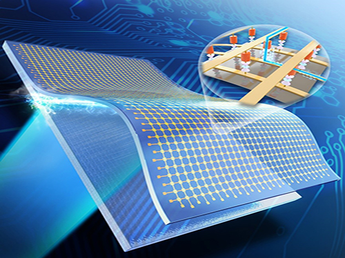
Picture 1: Artistic Rendtition of Light Interaction with Nanomaterials
(This image shows flash-induced plasmonic interactions with nanowires to improve silver nanowires (Ag NWs).)
Picture 2: Ag NW/PET Film
(This picture shows the Ag NWs on a polyethylene terephthalate (PET) film after the flash-induced plasmonic thermal process.)
2017.04.05 View 8335
Improving Silver Nanowires for FTCEs with Flash Light Interactions
Flexible transparent conducting electrodes (FTCEs) are an essential element of flexible optoelectronics for next-generation wearable displays, augmented reality (AR), and the Internet of Things (IoTs). Silver nanowires (Ag NWs) have received a great deal of attention as future FTCEs due to their great flexibility, material stability, and large-scale productivity. Despite these advantages, Ag NWs have drawbacks such as high wire-to-wire contact resistance and poor adhesion to substrates, resulting in severe power consumption and the delamination of FTCEs.
A research team led by Professor Keon Jae Lee of the Materials Science and Engineering Department at KAIST and Dr. Hong-Jin Park from BSP Inc., has developed high-performance Ag NWs (sheet resistance ~ 5 Ω/sq, transmittance 90 % at λ = 550 nm) with strong adhesion on plastic (interfacial energy of 30.7 J∙m-2) using flash light-material interactions.
The broad ultraviolet (UV) spectrum of a flash light enables the localized heating at the junctions of nanowires (NWs), which results in the fast and complete welding of Ag NWs. Consequently, the Ag NWs demonstrate six times higher conductivity than that of the pristine NWs. In addition, the near-infrared (NIR) of the flash lamp melted the interface between the Ag NWs and a polyethylene terephthalate (PET) substrate, dramatically enhancing the adhesion force of the Ag NWs to the PET by 310 %.
Professor Lee said, “Light interaction with nanomaterials is an important field for future flexible electronics since it can overcome thermal limit of plastics, and we are currently expanding our research into light-inorganic interactions.”
Meanwhile, BSP Inc., a laser manufacturing company and a collaborator of this work, has launched new flash lamp equipment for flexible applications based on the Professor Lee’s research.
The results of this work entitled “Flash-Induced Self-Limited Plasmonic Welding of Ag NW Network for Transparent Flexible Energy Harvester (DOI: 10.1002/adma.201603473)” were published in the February 2, 2017 issue of Advanced Materials as the cover article.
Professor Lee also contributed an invited review in the same journal of the April 3, 2017 online issue, “Laser-Material Interactions for Flexible Applications (DOI:10.1002/adma.201606586),” overviewing the recent advances in light interactions with flexible nanomaterials.
References
[1] Advanced Materials, February 2, 2017, Flash-Induced Self-Limited Plasmonic Welding of Ag NW network for Transparent Flexible Energy Harvester http://onlinelibrary.wiley.com/doi/10.1002/adma.201603473/epdf
[2] Advanced Materials, April 3, 2017, Laser-Material Interactions for Flexible Applications
http://onlinelibrary.wiley.com/doi/10.1002/adma.201606586/abstract
For further inquiries on research:
keonlee@kaist.ac.kr (Keon Jae Lee), hjpark@bsptech.co.kr (Hong-Jin Park)
Picture 1: Artistic Rendtition of Light Interaction with Nanomaterials
(This image shows flash-induced plasmonic interactions with nanowires to improve silver nanowires (Ag NWs).)
Picture 2: Ag NW/PET Film
(This picture shows the Ag NWs on a polyethylene terephthalate (PET) film after the flash-induced plasmonic thermal process.)
2017.04.05 View 8335 -
 Making Graphene Using Laser-induced Phase Separation
IBS & KAIST researchers clarify how laser annealing technology can lead to the production of ultrathin nanomaterials
All our smart phones have shiny flat AMOLED (active-matrix organic light-emitting diode) displays. Behind each single pixel of these displays hides at least two silicon transistors which are mass-manufactured using laser annealing technology. While the traditional methods to make the transistors use temperature above 1,000°C, the laser technique reaches the same results at low temperatures even on plastic substrates (melting temperature below 300°C). Interestingly, a similar procedure can be used to generate crystals of graphene. Graphene is a strong and thin nano-material made of carbon, its electric and heat-conductive properties have attracted the attention of scientists worldwide.
Professor Keon Jae Lee of the Materials Science and Engineering Department at KAIST and his research group at the Center for Multidimensional Carbon Materials within the Institute for Basic Science (IBS), as well as Professor Sung-Yool Choi of the Electrical Engineering School at KAIST and his research team discovered graphene synthesis mechanism using laser-induced solid-state phase separation of single-crystal silicon carbide (SiC). This study, available in Nature Communications, clarifies how this laser technology can separate a complex compound (SiC) into its ultrathin elements of carbon and silicon.
Although several fundamental studies presented the effect of excimer lasers in transforming elemental materials like silicon, the laser interaction with more complex compounds like SiC has rarely been studied due to the complexity of compound phase transition and ultra-short processing time.
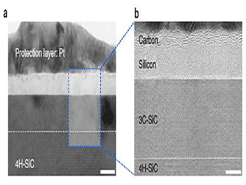
With high resolution microscope images and molecular dynamic simulations, scientists found that a single-pulse irradiation of xenon chloride excimer laser of 30 nanoseconds melts SiC, leading to the separation of a liquid SiC layer, a disordered carbon layer with graphitic domains (about 2.5 nm thick) on top surface and a polycrystalline silicon layer (about 5 nm) below carbon layer. Giving additional pulses causes the sublimation of the separated silicon, while the disordered carbon layer is transformed into a multilayer graphene.
"This research shows that the laser material interaction technology can be a powerful tool for the next generation of two dimensional nanomaterials," said Professor Lee.
Professor Choi added: "Using laser-induced phase separation of complex compounds, new types of two dimensional materials can be synthesized in the future."
High-resolution transmission electron microscopy shows that after just one laser pulse of 30 nanoseconds, the silicon carbide (SiC) substrate is melted and separates into a carbon and a silicon layer. More pulses cause the carbon layer to organize into graphene and the silicon to leave as gas.
Molecular dynamics simulates the graphene formation mechanism. The carbon layer on the top forms because the laser-induced liquid SiC (SiC (l)) is unstable.
(Press Release by Courtesy of the Institute for Basic Science (IBS))
2016.12.01 View 8598
Making Graphene Using Laser-induced Phase Separation
IBS & KAIST researchers clarify how laser annealing technology can lead to the production of ultrathin nanomaterials
All our smart phones have shiny flat AMOLED (active-matrix organic light-emitting diode) displays. Behind each single pixel of these displays hides at least two silicon transistors which are mass-manufactured using laser annealing technology. While the traditional methods to make the transistors use temperature above 1,000°C, the laser technique reaches the same results at low temperatures even on plastic substrates (melting temperature below 300°C). Interestingly, a similar procedure can be used to generate crystals of graphene. Graphene is a strong and thin nano-material made of carbon, its electric and heat-conductive properties have attracted the attention of scientists worldwide.
Professor Keon Jae Lee of the Materials Science and Engineering Department at KAIST and his research group at the Center for Multidimensional Carbon Materials within the Institute for Basic Science (IBS), as well as Professor Sung-Yool Choi of the Electrical Engineering School at KAIST and his research team discovered graphene synthesis mechanism using laser-induced solid-state phase separation of single-crystal silicon carbide (SiC). This study, available in Nature Communications, clarifies how this laser technology can separate a complex compound (SiC) into its ultrathin elements of carbon and silicon.
Although several fundamental studies presented the effect of excimer lasers in transforming elemental materials like silicon, the laser interaction with more complex compounds like SiC has rarely been studied due to the complexity of compound phase transition and ultra-short processing time.
With high resolution microscope images and molecular dynamic simulations, scientists found that a single-pulse irradiation of xenon chloride excimer laser of 30 nanoseconds melts SiC, leading to the separation of a liquid SiC layer, a disordered carbon layer with graphitic domains (about 2.5 nm thick) on top surface and a polycrystalline silicon layer (about 5 nm) below carbon layer. Giving additional pulses causes the sublimation of the separated silicon, while the disordered carbon layer is transformed into a multilayer graphene.
"This research shows that the laser material interaction technology can be a powerful tool for the next generation of two dimensional nanomaterials," said Professor Lee.
Professor Choi added: "Using laser-induced phase separation of complex compounds, new types of two dimensional materials can be synthesized in the future."
High-resolution transmission electron microscopy shows that after just one laser pulse of 30 nanoseconds, the silicon carbide (SiC) substrate is melted and separates into a carbon and a silicon layer. More pulses cause the carbon layer to organize into graphene and the silicon to leave as gas.
Molecular dynamics simulates the graphene formation mechanism. The carbon layer on the top forms because the laser-induced liquid SiC (SiC (l)) is unstable.
(Press Release by Courtesy of the Institute for Basic Science (IBS))
2016.12.01 View 8598 -
 Continuous Roll-Process Technology for Transferring and Packaging Flexible Large-Scale Integrated Circuits
A research team led by Professor Keon Jae Lee from KAIST and by Dr. Jae-Hyun Kim from the Korea Institute of Machinery and Materials (KIMM) has jointly developed a continuous roll-processing technology that transfers and packages flexible large-scale integrated circuits (LSI), the key element in constructing the computer’s brain such as CPU, on plastics to realize flexible electronics.
Professor Lee previously demonstrated the silicon-based flexible LSIs using 0.18 CMOS (complementary metal-oxide semiconductor) process in 2013 (ACS Nano, “In Vivo Silicon-based Flexible Radio Frequency Integrated Circuits Monolithically Encapsulated with Biocompatible Liquid Crystal Polymers”) and presented the work in an invited talk of 2015 International Electron Device Meeting (IEDM), the world’s premier semiconductor forum.
Highly productive roll-processing is considered a core technology for accelerating the commercialization of wearable computers using flexible LSI. However, realizing it has been a difficult challenge not only from the roll-based manufacturing perspective but also for creating roll-based packaging for the interconnection of flexible LSI with flexible displays, batteries, and other peripheral devices.
To overcome these challenges, the research team started fabricating NAND flash memories on a silicon wafer using conventional semiconductor processes, and then removed a sacrificial wafer leaving a top hundreds-nanometer-thick circuit layer. Next, they simultaneously transferred and interconnected the ultrathin device on a flexible substrate through the continuous roll-packaging technology using anisotropic conductive film (ACF). The final silicon-based flexible NAND memory successfully demonstrated stable memory operations and interconnections even under severe bending conditions. This roll-based flexible LSI technology can be potentially utilized to produce flexible application processors (AP), high-density memories, and high-speed communication devices for mass manufacture.
Professor Lee said, “Highly productive roll-process was successfully applied to flexible LSIs to continuously transfer and interconnect them onto plastics. For example, we have confirmed the reliable operation of our flexible NAND memory at the circuit level by programming and reading letters in ASCII codes. Out results may open up new opportunities to integrate silicon-based flexible LSIs on plastics with the ACF packing for roll-based manufacturing.”
Dr. Kim added, “We employed the roll-to-plate ACF packaging, which showed outstanding bonding capability for continuous roll-based transfer and excellent flexibility of interconnecting core and peripheral devices. This can be a key process to the new era of flexible computers combining the already developed flexible displays and batteries.”
The team’s results will be published on the front cover of Advanced Materials (August 31, 2016) in an article entitled “Simultaneous Roll Transfer and Interconnection of Silicon NAND Flash Memory.” (DOI: 10.1002/adma.201602339)
YouTube Link: https://www.youtube.com/watch?v=8OJjAEm27sw
Picture 1: This schematic image shows the flexible silicon NAND flash memory produced by the simultaneous roll-transfer and interconnection process.
Picture 2: The flexible silicon NAND flash memory is attached to a 7 mm diameter glass rod.
2016.09.01 View 8705
Continuous Roll-Process Technology for Transferring and Packaging Flexible Large-Scale Integrated Circuits
A research team led by Professor Keon Jae Lee from KAIST and by Dr. Jae-Hyun Kim from the Korea Institute of Machinery and Materials (KIMM) has jointly developed a continuous roll-processing technology that transfers and packages flexible large-scale integrated circuits (LSI), the key element in constructing the computer’s brain such as CPU, on plastics to realize flexible electronics.
Professor Lee previously demonstrated the silicon-based flexible LSIs using 0.18 CMOS (complementary metal-oxide semiconductor) process in 2013 (ACS Nano, “In Vivo Silicon-based Flexible Radio Frequency Integrated Circuits Monolithically Encapsulated with Biocompatible Liquid Crystal Polymers”) and presented the work in an invited talk of 2015 International Electron Device Meeting (IEDM), the world’s premier semiconductor forum.
Highly productive roll-processing is considered a core technology for accelerating the commercialization of wearable computers using flexible LSI. However, realizing it has been a difficult challenge not only from the roll-based manufacturing perspective but also for creating roll-based packaging for the interconnection of flexible LSI with flexible displays, batteries, and other peripheral devices.
To overcome these challenges, the research team started fabricating NAND flash memories on a silicon wafer using conventional semiconductor processes, and then removed a sacrificial wafer leaving a top hundreds-nanometer-thick circuit layer. Next, they simultaneously transferred and interconnected the ultrathin device on a flexible substrate through the continuous roll-packaging technology using anisotropic conductive film (ACF). The final silicon-based flexible NAND memory successfully demonstrated stable memory operations and interconnections even under severe bending conditions. This roll-based flexible LSI technology can be potentially utilized to produce flexible application processors (AP), high-density memories, and high-speed communication devices for mass manufacture.
Professor Lee said, “Highly productive roll-process was successfully applied to flexible LSIs to continuously transfer and interconnect them onto plastics. For example, we have confirmed the reliable operation of our flexible NAND memory at the circuit level by programming and reading letters in ASCII codes. Out results may open up new opportunities to integrate silicon-based flexible LSIs on plastics with the ACF packing for roll-based manufacturing.”
Dr. Kim added, “We employed the roll-to-plate ACF packaging, which showed outstanding bonding capability for continuous roll-based transfer and excellent flexibility of interconnecting core and peripheral devices. This can be a key process to the new era of flexible computers combining the already developed flexible displays and batteries.”
The team’s results will be published on the front cover of Advanced Materials (August 31, 2016) in an article entitled “Simultaneous Roll Transfer and Interconnection of Silicon NAND Flash Memory.” (DOI: 10.1002/adma.201602339)
YouTube Link: https://www.youtube.com/watch?v=8OJjAEm27sw
Picture 1: This schematic image shows the flexible silicon NAND flash memory produced by the simultaneous roll-transfer and interconnection process.
Picture 2: The flexible silicon NAND flash memory is attached to a 7 mm diameter glass rod.
2016.09.01 View 8705 -
 KAIST Develops Transparent Oxide Thin-Film Transistors
With the advent of the Internet of Things (IoT) era, strong demand has grown for wearable and transparent displays that can be applied to various fields such as augmented reality (AR) and skin-like thin flexible devices. However, previous flexible transparent displays have posed real challenges to overcome, which are, among others, poor transparency and low electrical performance. To improve the transparency and performance, past research efforts have tried to use inorganic-based electronics, but the fundamental thermal instabilities of plastic substrates have hampered the high temperature process, an essential step necessary for the fabrication of high performance electronic devices.
As a solution to this problem, a research team led by Professors Keon Jae Lee and Sang-Hee Ko Park of the Department of Materials Science and Engineering at the KAIST has developed ultrathin and transparent oxide thin-film transistors (TFT) for an active-matrix backplane of a flexible display by using the inorganic-based laser lift-off (ILLO) method. Professor Lee’s team previously demonstrated the ILLO technology for energy-harvesting (Advanced Materials, February 12, 2014) and flexible memory (Advanced Materials, September 8, 2014) devices.
The research team fabricated a high-performance oxide TFT array on top of a sacrificial laser-reactive substrate. After laser irradiation from the backside of the substrate, only the oxide TFT arrays were separated from the sacrificial substrate as a result of reaction between laser and laser-reactive layer, and then subsequently transferred onto ultrathin plastics ( thickness). Finally, the transferred ultrathin-oxide driving circuit for the flexible display was attached conformally to the surface of human skin to demonstrate the possibility of the wearable application. The attached oxide TFTs showed high optical transparency of 83% and mobility of even under several cycles of severe bending tests.
Professor Lee said, “By using our ILLO process, the technological barriers for high performance transparent flexible displays have been overcome at a relatively low cost by removing expensive polyimide substrates. Moreover, the high-quality oxide semiconductor can be easily transferred onto skin-like or any flexible substrate for wearable application.”
These research results, entitled “Skin-Like Oxide Thin-Film Transistors for Transparent Displays,”
(http://onlinelibrary.wiley.com/doi/10.1002/adfm.201601296/abstract) were the lead article published in the July 2016 online issue of Wiley’s Advanced Functional Materials.
###
References
[1] Advanced Materials, February 12, 2014, Highly-efficient, Flexible Piezoelectric PZT Thin Film Nanogenerator on Plastic Substrates
(http://onlinelibrary.wiley.com/doi/10.1002/adma.201305659/abstract)
[2] Advanced Materials, September 8, 2014, Flexible Crossbar-structured Resistive Memory Arrays on Plastic Substartes via Inorganic-based Laser Lift-off
(http://onlinelibrary.wiley.com/doi/10.1002/adma.201402472/abstract)
Picture 1: A Schamatic Image of Ultrathin, Flexible, and Transparent Oxide Thin-film Transistors
This image shows ultrathin, flexible, and transparent oxide thin-film transistors produced via the ILLO process.
Picture 2: Application of Uultrathin, Flexible, and Transparent Oxide Thin-film Transistors
This picture shows ultrathin, flexible, and transparent oxide thin-film transistors attached to a jumper sleeve and human skin.
2016.08.01 View 10415
KAIST Develops Transparent Oxide Thin-Film Transistors
With the advent of the Internet of Things (IoT) era, strong demand has grown for wearable and transparent displays that can be applied to various fields such as augmented reality (AR) and skin-like thin flexible devices. However, previous flexible transparent displays have posed real challenges to overcome, which are, among others, poor transparency and low electrical performance. To improve the transparency and performance, past research efforts have tried to use inorganic-based electronics, but the fundamental thermal instabilities of plastic substrates have hampered the high temperature process, an essential step necessary for the fabrication of high performance electronic devices.
As a solution to this problem, a research team led by Professors Keon Jae Lee and Sang-Hee Ko Park of the Department of Materials Science and Engineering at the KAIST has developed ultrathin and transparent oxide thin-film transistors (TFT) for an active-matrix backplane of a flexible display by using the inorganic-based laser lift-off (ILLO) method. Professor Lee’s team previously demonstrated the ILLO technology for energy-harvesting (Advanced Materials, February 12, 2014) and flexible memory (Advanced Materials, September 8, 2014) devices.
The research team fabricated a high-performance oxide TFT array on top of a sacrificial laser-reactive substrate. After laser irradiation from the backside of the substrate, only the oxide TFT arrays were separated from the sacrificial substrate as a result of reaction between laser and laser-reactive layer, and then subsequently transferred onto ultrathin plastics ( thickness). Finally, the transferred ultrathin-oxide driving circuit for the flexible display was attached conformally to the surface of human skin to demonstrate the possibility of the wearable application. The attached oxide TFTs showed high optical transparency of 83% and mobility of even under several cycles of severe bending tests.
Professor Lee said, “By using our ILLO process, the technological barriers for high performance transparent flexible displays have been overcome at a relatively low cost by removing expensive polyimide substrates. Moreover, the high-quality oxide semiconductor can be easily transferred onto skin-like or any flexible substrate for wearable application.”
These research results, entitled “Skin-Like Oxide Thin-Film Transistors for Transparent Displays,”
(http://onlinelibrary.wiley.com/doi/10.1002/adfm.201601296/abstract) were the lead article published in the July 2016 online issue of Wiley’s Advanced Functional Materials.
###
References
[1] Advanced Materials, February 12, 2014, Highly-efficient, Flexible Piezoelectric PZT Thin Film Nanogenerator on Plastic Substrates
(http://onlinelibrary.wiley.com/doi/10.1002/adma.201305659/abstract)
[2] Advanced Materials, September 8, 2014, Flexible Crossbar-structured Resistive Memory Arrays on Plastic Substartes via Inorganic-based Laser Lift-off
(http://onlinelibrary.wiley.com/doi/10.1002/adma.201402472/abstract)
Picture 1: A Schamatic Image of Ultrathin, Flexible, and Transparent Oxide Thin-film Transistors
This image shows ultrathin, flexible, and transparent oxide thin-film transistors produced via the ILLO process.
Picture 2: Application of Uultrathin, Flexible, and Transparent Oxide Thin-film Transistors
This picture shows ultrathin, flexible, and transparent oxide thin-film transistors attached to a jumper sleeve and human skin.
2016.08.01 View 10415 -
 KAIST Team Develops Flexible PRAM
Phase change random access memory (PRAM) is one of the strongest candidates for next-generation nonvolatile memory for flexible and wearable electronics. In order to be used as a core memory for flexible devices, the most important issue is reducing high operating current. The effective solution is to decrease cell size in sub-micron region as in commercialized conventional PRAM. However, the scaling to nano-dimension on flexible substrates is extremely difficult due to soft nature and photolithographic limits on plastics, thus practical flexible PRAM has not been realized yet.
Recently, a team led by Professors Keon Jae Lee and Yeon Sik Jung of the Department of Materials Science and Engineering at KAIST has developed the first flexible PRAM enabled by self-assembled block copolymer (BCP) silica nanostructures with an ultralow current operation (below one quarter of conventional PRAM without BCP) on plastic substrates. BCP is the mixture of two different polymer materials, which can easily create self-ordered arrays of sub-20 nm features through simple spin-coating and plasma treatments. BCP silica nanostructures successfully lowered the contact area by localizing the volume change of phase-change materials and thus resulted in significant power reduction. Furthermore, the ultrathin silicon-based diodes were integrated with phase-change memories (PCM) to suppress the inter-cell interference, which demonstrated random access capability for flexible and wearable electronics. Their work was published in the March issue of ACS Nano: "Flexible One Diode-One Phase Change Memory Array Enabled by Block Copolymer Self-Assembly."
Another way to achieve ultralow-powered PRAM is to utilize self-structured conductive filaments (CF) instead of the resistor-type conventional heater. The self-structured CF nanoheater originated from unipolar memristor can generate strong heat toward phase-change materials due to high current density through the nanofilament. This ground-breaking methodology shows that sub-10 nm filament heater, without using expensive and non-compatible nanolithography, achieved nanoscale switching volume of phase change materials, resulted in the PCM writing current of below 20 uA, the lowest value among top-down PCM devices. This achievement was published in the June online issue of ACS Nano: "Self-Structured Conductive Filament Nanoheater for Chalcogenide Phase Transition." In addition, due to self-structured low-power technology compatible to plastics, the research team has recently succeeded in fabricating a flexible PRAM on wearable substrates.
Professor Lee said, "The demonstration of low power PRAM on plastics is one of the most important issues for next-generation wearable and flexible non-volatile memory. Our innovative and simple methodology represents the strong potential for commercializing flexible PRAM."
In addition, he wrote a review paper regarding the nanotechnology-based electronic devices in the June online issue of Advanced Materials entitled "Performance Enhancement of Electronic and Energy Devices via Block Copolymer Self-Assembly."
Picture Caption:
Low-power nonvolatile PRAM for flexible and wearable memories enabled by (a) self-assembled BCP silica nanostructures and (b) self-structured conductive filament nanoheater.
2015.06.15 View 13088
KAIST Team Develops Flexible PRAM
Phase change random access memory (PRAM) is one of the strongest candidates for next-generation nonvolatile memory for flexible and wearable electronics. In order to be used as a core memory for flexible devices, the most important issue is reducing high operating current. The effective solution is to decrease cell size in sub-micron region as in commercialized conventional PRAM. However, the scaling to nano-dimension on flexible substrates is extremely difficult due to soft nature and photolithographic limits on plastics, thus practical flexible PRAM has not been realized yet.
Recently, a team led by Professors Keon Jae Lee and Yeon Sik Jung of the Department of Materials Science and Engineering at KAIST has developed the first flexible PRAM enabled by self-assembled block copolymer (BCP) silica nanostructures with an ultralow current operation (below one quarter of conventional PRAM without BCP) on plastic substrates. BCP is the mixture of two different polymer materials, which can easily create self-ordered arrays of sub-20 nm features through simple spin-coating and plasma treatments. BCP silica nanostructures successfully lowered the contact area by localizing the volume change of phase-change materials and thus resulted in significant power reduction. Furthermore, the ultrathin silicon-based diodes were integrated with phase-change memories (PCM) to suppress the inter-cell interference, which demonstrated random access capability for flexible and wearable electronics. Their work was published in the March issue of ACS Nano: "Flexible One Diode-One Phase Change Memory Array Enabled by Block Copolymer Self-Assembly."
Another way to achieve ultralow-powered PRAM is to utilize self-structured conductive filaments (CF) instead of the resistor-type conventional heater. The self-structured CF nanoheater originated from unipolar memristor can generate strong heat toward phase-change materials due to high current density through the nanofilament. This ground-breaking methodology shows that sub-10 nm filament heater, without using expensive and non-compatible nanolithography, achieved nanoscale switching volume of phase change materials, resulted in the PCM writing current of below 20 uA, the lowest value among top-down PCM devices. This achievement was published in the June online issue of ACS Nano: "Self-Structured Conductive Filament Nanoheater for Chalcogenide Phase Transition." In addition, due to self-structured low-power technology compatible to plastics, the research team has recently succeeded in fabricating a flexible PRAM on wearable substrates.
Professor Lee said, "The demonstration of low power PRAM on plastics is one of the most important issues for next-generation wearable and flexible non-volatile memory. Our innovative and simple methodology represents the strong potential for commercializing flexible PRAM."
In addition, he wrote a review paper regarding the nanotechnology-based electronic devices in the June online issue of Advanced Materials entitled "Performance Enhancement of Electronic and Energy Devices via Block Copolymer Self-Assembly."
Picture Caption:
Low-power nonvolatile PRAM for flexible and wearable memories enabled by (a) self-assembled BCP silica nanostructures and (b) self-structured conductive filament nanoheater.
2015.06.15 View 13088 -
 KAIST Researchers Develops Hyper-Stretchable Elastic-Composite Energy Harvester
A research team led by Professor Keon Jae Lee (http://fand.kaist.ac.kr) of the Department of Materials Science and Engineering at KAIST has developed a hyper-stretchable elastic-composite energy harvesting device called a nanogenerator.
Flexible electronics have come into the market and are enabling new technologies like flexible displays in mobile phone, wearable electronics, and the Internet of Things (IoTs). However, is the degree of flexibility enough for most applications? For many flexible devices, elasticity is a very important issue. For example, wearable/biomedical devices and electronic skins (e-skins) should stretch to conform to arbitrarily curved surfaces and moving body parts such as joints, diaphragms, and tendons. They must be able to withstand the repeated and prolonged mechanical stresses of stretching. In particular, the development of elastic energy devices is regarded as critical to establish power supplies in stretchable applications. Although several researchers have explored diverse stretchable electronics, due to the absence of the appropriate device structures and correspondingly electrodes, researchers have not developed ultra-stretchable and fully-reversible energy conversion devices properly.
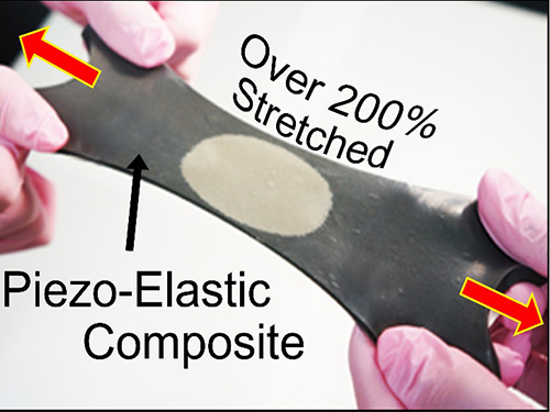
Recently, researchers from KAIST and Seoul National University (SNU) have collaborated and demonstrated a facile methodology to obtain a high-performance and hyper-stretchable elastic-composite generator (SEG) using very long silver nanowire-based stretchable electrodes. Their stretchable piezoelectric generator can harvest mechanical energy to produce high power output (~4 V) with large elasticity (~250%) and excellent durability (over 104 cycles). These noteworthy results were achieved by the non-destructive stress- relaxation ability of the unique electrodes as well as the good piezoelectricity of the device components. The new SEG can be applied to a wide-variety of wearable energy-harvesters to transduce biomechanical-stretching energy from the body (or machines) to electrical energy.
Professor Lee said, “This exciting approach introduces an ultra-stretchable piezoelectric generator. It can open avenues for power supplies in universal wearable and biomedical applications as well as self-powered ultra-stretchable electronics.”
This result was published online in the March issue of Advanced Materials, which is entitled “A Hyper-Stretchable Elastic-Composite Energy Harvester.”
YouTube Link: “A hyper-stretchable energy harvester”
https://www.youtube.com/watch?v=EBByFvPVRiU&feature=youtu.be
Figure: Top row: Schematics of hyper-stretchable elastic-composite generator enabled by very long silver nanowire-based stretchable electrodes.
Bottom row: The SEG energy harvester stretched by human hands over 200% strain.
2015.04.14 View 11742
KAIST Researchers Develops Hyper-Stretchable Elastic-Composite Energy Harvester
A research team led by Professor Keon Jae Lee (http://fand.kaist.ac.kr) of the Department of Materials Science and Engineering at KAIST has developed a hyper-stretchable elastic-composite energy harvesting device called a nanogenerator.
Flexible electronics have come into the market and are enabling new technologies like flexible displays in mobile phone, wearable electronics, and the Internet of Things (IoTs). However, is the degree of flexibility enough for most applications? For many flexible devices, elasticity is a very important issue. For example, wearable/biomedical devices and electronic skins (e-skins) should stretch to conform to arbitrarily curved surfaces and moving body parts such as joints, diaphragms, and tendons. They must be able to withstand the repeated and prolonged mechanical stresses of stretching. In particular, the development of elastic energy devices is regarded as critical to establish power supplies in stretchable applications. Although several researchers have explored diverse stretchable electronics, due to the absence of the appropriate device structures and correspondingly electrodes, researchers have not developed ultra-stretchable and fully-reversible energy conversion devices properly.
Recently, researchers from KAIST and Seoul National University (SNU) have collaborated and demonstrated a facile methodology to obtain a high-performance and hyper-stretchable elastic-composite generator (SEG) using very long silver nanowire-based stretchable electrodes. Their stretchable piezoelectric generator can harvest mechanical energy to produce high power output (~4 V) with large elasticity (~250%) and excellent durability (over 104 cycles). These noteworthy results were achieved by the non-destructive stress- relaxation ability of the unique electrodes as well as the good piezoelectricity of the device components. The new SEG can be applied to a wide-variety of wearable energy-harvesters to transduce biomechanical-stretching energy from the body (or machines) to electrical energy.
Professor Lee said, “This exciting approach introduces an ultra-stretchable piezoelectric generator. It can open avenues for power supplies in universal wearable and biomedical applications as well as self-powered ultra-stretchable electronics.”
This result was published online in the March issue of Advanced Materials, which is entitled “A Hyper-Stretchable Elastic-Composite Energy Harvester.”
YouTube Link: “A hyper-stretchable energy harvester”
https://www.youtube.com/watch?v=EBByFvPVRiU&feature=youtu.be
Figure: Top row: Schematics of hyper-stretchable elastic-composite generator enabled by very long silver nanowire-based stretchable electrodes.
Bottom row: The SEG energy harvester stretched by human hands over 200% strain.
2015.04.14 View 11742 -
 Breakthrough in Flexible Electronics Enabled by Inorganic-based Laser Lift-off
Flexible electronics have been touted as the next generation in electronics in various areas, ranging from consumer electronics to bio-integrated medical devices. In spite of their merits, insufficient performance of organic materials arising from inherent material properties and processing limitations in scalability have posed big challenges to developing all-in-one flexible electronics systems in which display, processor, memory, and energy devices are integrated. The high temperature processes, essential for high performance electronic devices, have severely restricted the development of flexible electronics because of the fundamental thermal instabilities of polymer materials.
A research team headed by Professor Keon Jae Lee of the Department of Materials Science and Engineering at KAIST provides an easier methodology to realize high performance flexible electronics by using the Inorganic-based Laser Lift-off (ILLO).
The ILLO process involves depositing a laser-reactive exfoliation layer on rigid substrates, and then fabricating ultrathin inorganic electronic devices, e.g., high density crossbar memristive memory on top of the exfoliation layer. By laser irradiation through the back of the substrate, only the ultrathin inorganic device layers are exfoliated from the substrate as a result of the reaction between laser and exfoliation layer, and then subsequently transferred onto any kind of receiver substrate such as plastic, paper, and even fabric.
This ILLO process can enable not only nanoscale processes for high density flexible devices but also the high temperature process that was previously difficult to achieve on plastic substrates. The transferred device successfully demonstrates fully-functional random access memory operation on flexible substrates even under severe bending.
Professor Lee said, “By selecting an optimized set of inorganic exfoliation layer and substrate, a nanoscale process at a high temperature of over 1000 °C can be utilized for high performance flexible electronics. The ILLO process can be applied to diverse flexible electronics, such as driving circuits for displays and inorganic-based energy devices such as battery, solar cell, and self-powered devices that require high temperature processes.”
The team’s results were published in the November issue of Wiley’s journal, ‘ Advanced Materials, ’ as a cover article entitled “ Flexible Crossbar-Structured Resistive Memory Arrays on Plastic Substrates via Inorganic-Based Laser Lift-Off.”
( http://onlinelibrary.wiley.com/doi/10.1002/adma.201402472/abstract )
This schematic picture shows the flexible crossbar memory developed via the ILLO process.
This photo shows the flexible RRAM device on a plastic substrate.
2014.11.26 View 8730
Breakthrough in Flexible Electronics Enabled by Inorganic-based Laser Lift-off
Flexible electronics have been touted as the next generation in electronics in various areas, ranging from consumer electronics to bio-integrated medical devices. In spite of their merits, insufficient performance of organic materials arising from inherent material properties and processing limitations in scalability have posed big challenges to developing all-in-one flexible electronics systems in which display, processor, memory, and energy devices are integrated. The high temperature processes, essential for high performance electronic devices, have severely restricted the development of flexible electronics because of the fundamental thermal instabilities of polymer materials.
A research team headed by Professor Keon Jae Lee of the Department of Materials Science and Engineering at KAIST provides an easier methodology to realize high performance flexible electronics by using the Inorganic-based Laser Lift-off (ILLO).
The ILLO process involves depositing a laser-reactive exfoliation layer on rigid substrates, and then fabricating ultrathin inorganic electronic devices, e.g., high density crossbar memristive memory on top of the exfoliation layer. By laser irradiation through the back of the substrate, only the ultrathin inorganic device layers are exfoliated from the substrate as a result of the reaction between laser and exfoliation layer, and then subsequently transferred onto any kind of receiver substrate such as plastic, paper, and even fabric.
This ILLO process can enable not only nanoscale processes for high density flexible devices but also the high temperature process that was previously difficult to achieve on plastic substrates. The transferred device successfully demonstrates fully-functional random access memory operation on flexible substrates even under severe bending.
Professor Lee said, “By selecting an optimized set of inorganic exfoliation layer and substrate, a nanoscale process at a high temperature of over 1000 °C can be utilized for high performance flexible electronics. The ILLO process can be applied to diverse flexible electronics, such as driving circuits for displays and inorganic-based energy devices such as battery, solar cell, and self-powered devices that require high temperature processes.”
The team’s results were published in the November issue of Wiley’s journal, ‘ Advanced Materials, ’ as a cover article entitled “ Flexible Crossbar-Structured Resistive Memory Arrays on Plastic Substrates via Inorganic-Based Laser Lift-Off.”
( http://onlinelibrary.wiley.com/doi/10.1002/adma.201402472/abstract )
This schematic picture shows the flexible crossbar memory developed via the ILLO process.
This photo shows the flexible RRAM device on a plastic substrate.
2014.11.26 View 8730 -
 President Steve Kang of KAIST Attends the 2014 Summer Davos Forum in Tianjin, China
President Steve Kang of KAIST will attend the 2014 Annual Meeting of the New Champions, the World Economic Forum (WEF), to be held on September 10-12, 2014 in Tianjin, China.
KAIST holds its own IdeasLab session on nanotechnology on September 12, 2014.
On September 10, 2014, President Steve Kang will participate in a private session hosted by the Global University Leaders Forum (GULF) community at WEF as a panelist.
In addition to President Kang, eight presidents from top global universities such as the National University of Singapore, Peking University, ETH Zurich (Swiss Federal Institute of Technology), University of Tokyo, and Carnegie Mellon University will join the panel discussion under the topic, “Increasing the Translational Impact of University Research.” Specifically, the presidents will address issues related to the importance of university-led technology transfer in Asia, key strategies and goals for technology transfer, and implementation approaches taken by each university to promote technology transfer from university to industry.
President Kang was invited to this GULF session, the only attendant from Korean universities, in recognition of his long time experience and expertise in education and research.
In 2006, WEF created the GULF, a small community of the presidents of top universities in the world, aiming to offer an open platform for high-level dialogues on issues of higher education and research with other sectors, as well as to foster collaboration between universities in areas of significance for global policy.
As of 2014, a total of 25 globally leading universities, including Harvard University, University of Cambridge, and Massachusetts Institute of Technology, are GULF members. KAIST, which joined the club this year, is the only Korean university.
The 2014 Annual Meeting of the New Champions, also known as the Summer Davos Forum, hosts numerous sessions under the theme of “Creating Value through Innovation.” At the Forum, a total of ten IdeasLab sessions will be hosted. KAIST was invited to run its own IdeasLab on nanotechnology on September 12, 2014.
Together with President Kang, Professors Sang Ouk Kim and Keon Jae Lee from the Department of Materials Science Engineering, KAIST, and Professors Sang Yup Lee and Hyunjoo Lee from the Department of Chemical and Biomolecular Engineering, KAIST, will present their own speeches on the topic entitled “From diagnostics to materials, how is nanotechnology changing lives?”
President Kang will give the opening speech at the KAIST IdeasLab.
He said that an invitation from WEF to join the IdeasLab spoke well for KAIST:
“KAIST is the first and the only Korean university ever invited to run its own IdeasLab at the World Economic Forum. The IdeasLab is an expert group meeting, conducted only by the world’s most prestigious universities and research institutes. At the IdeasLab sessions, global leaders from different sectors identify major issues facing higher education and humanity and explore solutions through science and technology innovation. Holding our own IdeasLab on one of our strongest fields, nanotechnology, is indeed an excellent opportunity for KAIST to show its strength in academic and research excellence on the global stage.”
2014.09.08 View 10807
President Steve Kang of KAIST Attends the 2014 Summer Davos Forum in Tianjin, China
President Steve Kang of KAIST will attend the 2014 Annual Meeting of the New Champions, the World Economic Forum (WEF), to be held on September 10-12, 2014 in Tianjin, China.
KAIST holds its own IdeasLab session on nanotechnology on September 12, 2014.
On September 10, 2014, President Steve Kang will participate in a private session hosted by the Global University Leaders Forum (GULF) community at WEF as a panelist.
In addition to President Kang, eight presidents from top global universities such as the National University of Singapore, Peking University, ETH Zurich (Swiss Federal Institute of Technology), University of Tokyo, and Carnegie Mellon University will join the panel discussion under the topic, “Increasing the Translational Impact of University Research.” Specifically, the presidents will address issues related to the importance of university-led technology transfer in Asia, key strategies and goals for technology transfer, and implementation approaches taken by each university to promote technology transfer from university to industry.
President Kang was invited to this GULF session, the only attendant from Korean universities, in recognition of his long time experience and expertise in education and research.
In 2006, WEF created the GULF, a small community of the presidents of top universities in the world, aiming to offer an open platform for high-level dialogues on issues of higher education and research with other sectors, as well as to foster collaboration between universities in areas of significance for global policy.
As of 2014, a total of 25 globally leading universities, including Harvard University, University of Cambridge, and Massachusetts Institute of Technology, are GULF members. KAIST, which joined the club this year, is the only Korean university.
The 2014 Annual Meeting of the New Champions, also known as the Summer Davos Forum, hosts numerous sessions under the theme of “Creating Value through Innovation.” At the Forum, a total of ten IdeasLab sessions will be hosted. KAIST was invited to run its own IdeasLab on nanotechnology on September 12, 2014.
Together with President Kang, Professors Sang Ouk Kim and Keon Jae Lee from the Department of Materials Science Engineering, KAIST, and Professors Sang Yup Lee and Hyunjoo Lee from the Department of Chemical and Biomolecular Engineering, KAIST, will present their own speeches on the topic entitled “From diagnostics to materials, how is nanotechnology changing lives?”
President Kang will give the opening speech at the KAIST IdeasLab.
He said that an invitation from WEF to join the IdeasLab spoke well for KAIST:
“KAIST is the first and the only Korean university ever invited to run its own IdeasLab at the World Economic Forum. The IdeasLab is an expert group meeting, conducted only by the world’s most prestigious universities and research institutes. At the IdeasLab sessions, global leaders from different sectors identify major issues facing higher education and humanity and explore solutions through science and technology innovation. Holding our own IdeasLab on one of our strongest fields, nanotechnology, is indeed an excellent opportunity for KAIST to show its strength in academic and research excellence on the global stage.”
2014.09.08 View 10807 -
 The First Demonstration of a Self-powered Cardiac Pacemaker
As the number of pacemakers implanted each year reaches into the millions worldwide, improving the lifespan of pacemaker batteries has been of great concern for developers and manufacturers. Currently, pacemaker batteries last seven years on average, requiring frequent replacements, which may pose patients to a potential risk involved in medical procedures.
A research team from the Korea Advanced Institute of Science and Technology (KAIST), headed by Professor Keon Jae Lee of the Department of Materials Science and Engineering at KAIST and Professor Boyoung Joung, M.D. of the Division of Cardiology at Severance Hospital of Yonsei University, has developed a self-powered artificial cardiac pacemaker that is operated semi-permanently by a flexible piezoelectric nanogenerator.
The artificial cardiac pacemaker is widely acknowledged as medical equipment that is integrated into the human body to regulate the heartbeats through electrical stimulation to contract the cardiac muscles of people who suffer from arrhythmia. However, repeated surgeries to replace pacemaker batteries have exposed elderly patients to health risks such as infections or severe bleeding during operations.
The team’s newly designed flexible piezoelectric nanogenerator directly stimulated a living rat’s heart using electrical energy converted from the small body movements of the rat. This technology could facilitate the use of self-powered flexible energy harvesters, not only prolonging the lifetime of cardiac pacemakers but also realizing real-time heart monitoring.
The research team fabricated high-performance flexible nanogenerators utilizing a bulk single-crystal PMN-PT thin film (iBULe Photonics). The harvested energy reached up to 8.2 V and 0.22 mA by bending and pushing motions, which were high enough values to directly stimulate the rat’s heart.
Professor Keon Jae Lee said:
“For clinical purposes, the current achievement will benefit the development of self-powered cardiac pacemakers as well as prevent heart attacks via the real-time diagnosis of heart arrhythmia. In addition, the flexible piezoelectric nanogenerator could also be utilized as an electrical source for various implantable medical devices.”
This research result was described in the April online issue of Advanced Materials (“Self-Powered Cardiac Pacemaker Enabled by Flexible Single Crystalline PMN-PT Piezoelectric Energy Harvester”: http://onlinelibrary.wiley.com/doi/10.1002/adma.201400562/abstract).
Youtube link: http://www.youtube.com/watch?v=ZWYT2cU_Mog&feature=youtu.be
Picture Caption: A self-powered cardiac pacemaker is enabled by a flexible piezoelectric energy harvester.
2014.06.25 View 14281
The First Demonstration of a Self-powered Cardiac Pacemaker
As the number of pacemakers implanted each year reaches into the millions worldwide, improving the lifespan of pacemaker batteries has been of great concern for developers and manufacturers. Currently, pacemaker batteries last seven years on average, requiring frequent replacements, which may pose patients to a potential risk involved in medical procedures.
A research team from the Korea Advanced Institute of Science and Technology (KAIST), headed by Professor Keon Jae Lee of the Department of Materials Science and Engineering at KAIST and Professor Boyoung Joung, M.D. of the Division of Cardiology at Severance Hospital of Yonsei University, has developed a self-powered artificial cardiac pacemaker that is operated semi-permanently by a flexible piezoelectric nanogenerator.
The artificial cardiac pacemaker is widely acknowledged as medical equipment that is integrated into the human body to regulate the heartbeats through electrical stimulation to contract the cardiac muscles of people who suffer from arrhythmia. However, repeated surgeries to replace pacemaker batteries have exposed elderly patients to health risks such as infections or severe bleeding during operations.
The team’s newly designed flexible piezoelectric nanogenerator directly stimulated a living rat’s heart using electrical energy converted from the small body movements of the rat. This technology could facilitate the use of self-powered flexible energy harvesters, not only prolonging the lifetime of cardiac pacemakers but also realizing real-time heart monitoring.
The research team fabricated high-performance flexible nanogenerators utilizing a bulk single-crystal PMN-PT thin film (iBULe Photonics). The harvested energy reached up to 8.2 V and 0.22 mA by bending and pushing motions, which were high enough values to directly stimulate the rat’s heart.
Professor Keon Jae Lee said:
“For clinical purposes, the current achievement will benefit the development of self-powered cardiac pacemakers as well as prevent heart attacks via the real-time diagnosis of heart arrhythmia. In addition, the flexible piezoelectric nanogenerator could also be utilized as an electrical source for various implantable medical devices.”
This research result was described in the April online issue of Advanced Materials (“Self-Powered Cardiac Pacemaker Enabled by Flexible Single Crystalline PMN-PT Piezoelectric Energy Harvester”: http://onlinelibrary.wiley.com/doi/10.1002/adma.201400562/abstract).
Youtube link: http://www.youtube.com/watch?v=ZWYT2cU_Mog&feature=youtu.be
Picture Caption: A self-powered cardiac pacemaker is enabled by a flexible piezoelectric energy harvester.
2014.06.25 View 14281 -
 KAIST Made Great Improvements of Nanogenerator Power Efficiency
The energy efficiency of a piezoelectric nanogenerator developed by KAIST has increased by almost 40 times, one step closer toward the commercialization of flexible energy harvesters that can supply power infinitely to wearable, implantable electronic devices.
NANOGENERATORS are innovative self-powered energy harvesters that convert kinetic energy created from vibrational and mechanical sources into electrical power, removing the need of external circuits or batteries for electronic devices. This innovation is vital in realizing sustainable energy generation in isolated, inaccessible, or indoor environments and even in the human body.
Nanogenerators, a flexible and lightweight energy harvester on a plastic substrate, can scavenge energy from the extremely tiny movements of natural resources and human body such as wind, water flow, heartbeats, and diaphragm and respiration activities to generate electrical signals. The generators are not only self-powered, flexible devices but also can provide permanent power sources to implantable biomedical devices, including cardiac pacemakers and deep brain stimulators.
However, poor energy efficiency and a complex fabrication process have posed challenges to the commercialization of nanogenerators. Keon Jae Lee, Associate Professor of Materials Science and Engineering at KAIST, and his colleagues have recently proposed a solution by developing a robust technique to transfer a high-quality piezoelectric thin film from bulk sapphire substrates to plastic substrates using laser lift-off (LLO).
Applying the inorganic-based laser lift-off (LLO) process, the research team produced a large-area PZT thin film nanogenerators on flexible substrates (2cm x 2cm).
“We were able to convert a high-output performance of ~250 V from the slight mechanical deformation of a single thin plastic substrate. Such output power is just enough to turn on 100 LED lights,” Keon Jae Lee explained.
The self-powered nanogenerators can also work with finger and foot motions. For example, under the irregular and slight bending motions of a human finger, the measured current signals had a high electric power of ~8.7 μA. In addition, the piezoelectric nanogenerator has world-record power conversion efficiency, almost 40 times higher than previously reported similar research results, solving the drawbacks related to the fabrication complexity and low energy efficiency.
Lee further commented,
“Building on this concept, it is highly expected that tiny mechanical motions, including human body movements of muscle contraction and relaxation, can be readily converted into electrical energy and, furthermore, acted as eternal power sources.”
The research team is currently studying a method to build three-dimensional stacking of flexible piezoelectric thin films to enhance output power, as well as conducting a clinical experiment with a flexible nanogenerator.
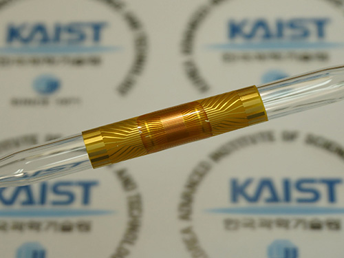
This research result, entitled “Highly-efficient, Flexible Piezoelectric PZT Thin Film Nanogenerator on Plastic Substrates,” was published as the cover article of the April issue of Advanced Materials. (http://onlinelibrary.wiley.com/doi/10.1002/adma.201305659/abstract)
YouTube Link: http://www.youtube.com/watch?v=G_Fny7Xb9ig
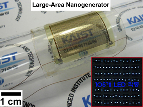
Over 100 LEDs operated by self-powered flexible piezoelectric thin film nanogenerator
Flexible PZT thin film nanogenerator using inorganic-based laser lift-off process
Photograph of large-area PZT thin film nanogenerator (3.5cm × 3.5cm) on a curved glass tube and 105 commercial LEDs operated by self-powered flexible piezoelectric energy harvester
2014.05.19 View 12133
KAIST Made Great Improvements of Nanogenerator Power Efficiency
The energy efficiency of a piezoelectric nanogenerator developed by KAIST has increased by almost 40 times, one step closer toward the commercialization of flexible energy harvesters that can supply power infinitely to wearable, implantable electronic devices.
NANOGENERATORS are innovative self-powered energy harvesters that convert kinetic energy created from vibrational and mechanical sources into electrical power, removing the need of external circuits or batteries for electronic devices. This innovation is vital in realizing sustainable energy generation in isolated, inaccessible, or indoor environments and even in the human body.
Nanogenerators, a flexible and lightweight energy harvester on a plastic substrate, can scavenge energy from the extremely tiny movements of natural resources and human body such as wind, water flow, heartbeats, and diaphragm and respiration activities to generate electrical signals. The generators are not only self-powered, flexible devices but also can provide permanent power sources to implantable biomedical devices, including cardiac pacemakers and deep brain stimulators.
However, poor energy efficiency and a complex fabrication process have posed challenges to the commercialization of nanogenerators. Keon Jae Lee, Associate Professor of Materials Science and Engineering at KAIST, and his colleagues have recently proposed a solution by developing a robust technique to transfer a high-quality piezoelectric thin film from bulk sapphire substrates to plastic substrates using laser lift-off (LLO).
Applying the inorganic-based laser lift-off (LLO) process, the research team produced a large-area PZT thin film nanogenerators on flexible substrates (2cm x 2cm).
“We were able to convert a high-output performance of ~250 V from the slight mechanical deformation of a single thin plastic substrate. Such output power is just enough to turn on 100 LED lights,” Keon Jae Lee explained.
The self-powered nanogenerators can also work with finger and foot motions. For example, under the irregular and slight bending motions of a human finger, the measured current signals had a high electric power of ~8.7 μA. In addition, the piezoelectric nanogenerator has world-record power conversion efficiency, almost 40 times higher than previously reported similar research results, solving the drawbacks related to the fabrication complexity and low energy efficiency.
Lee further commented,
“Building on this concept, it is highly expected that tiny mechanical motions, including human body movements of muscle contraction and relaxation, can be readily converted into electrical energy and, furthermore, acted as eternal power sources.”
The research team is currently studying a method to build three-dimensional stacking of flexible piezoelectric thin films to enhance output power, as well as conducting a clinical experiment with a flexible nanogenerator.
This research result, entitled “Highly-efficient, Flexible Piezoelectric PZT Thin Film Nanogenerator on Plastic Substrates,” was published as the cover article of the April issue of Advanced Materials. (http://onlinelibrary.wiley.com/doi/10.1002/adma.201305659/abstract)
YouTube Link: http://www.youtube.com/watch?v=G_Fny7Xb9ig
Over 100 LEDs operated by self-powered flexible piezoelectric thin film nanogenerator
Flexible PZT thin film nanogenerator using inorganic-based laser lift-off process
Photograph of large-area PZT thin film nanogenerator (3.5cm × 3.5cm) on a curved glass tube and 105 commercial LEDs operated by self-powered flexible piezoelectric energy harvester
2014.05.19 View 12133 -
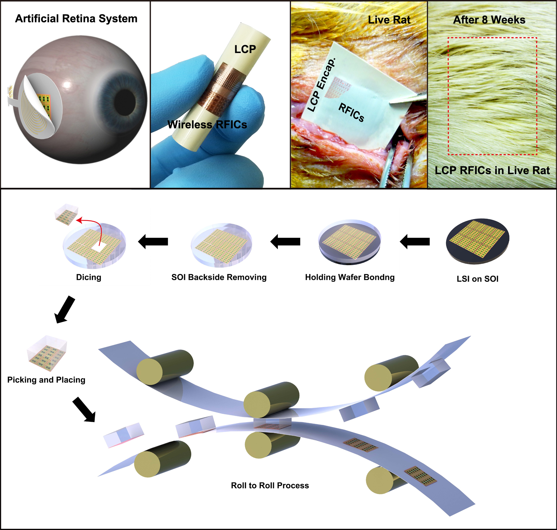 A KAIST research team developed in vivo flexible large scale integrated circuits
Daejeon, Republic of Korea, May 6th, 2013–-A team led by Professor Keon Jae Lee from the Department of Materials Science and Engineering at KAIST has developed in vivo silicon-based flexible large scale integrated circuits (LSI) for bio-medical wireless communication.
Silicon-based semiconductors have played significant roles in signal processing, nerve stimulation, memory storage, and wireless communication in implantable electronics. However, the rigid and bulky LSI chips have limited uses in in vivo devices due to incongruent contact with the curvilinear surfaces of human organs. Especially, artificial retinas recently approved by the Food and Drug Administration (refer to the press release of FDA"s artificial retina approval) require extremely flexible and slim LSI to incorporate it within the cramped area of the human eye.
Although several research teams have fabricated flexible integrated circuits (ICs, tens of interconnected transistors) on plastics, their inaccurate nano-scale alignment on plastics has restricted the demonstration of flexible nano-transistors and their large scale interconnection for in vivo LSI applications such as main process unit (MPU), high density memory and wireless communication. Professor Lee"s team previously demonstrated fully functional flexible memory using ultrathin silicon membranes (Nano Letters, Flexible Memristive Memory Array on Plastic Substrates), however, its integration level and transistor size (over micron scale) have limited functional applications for flexible consumer electronics.
Professor Keon Jae Lee"s team fabricated radio frequency integrated circuits (RFICs) interconnected with thousand nano-transistors on silicon wafer by state-of-the-art CMOS process, and then they removed the entire bottom substrate except top 100 nm active circuit layer by wet chemical etching. The flexible RF switches for wireless communication were monolithically encapsulated with biocompatible liquid crystal polymers (LCPs) for in vivo bio-medical applications. Finally, they implanted the LCP encapsulated RFICs into live rats to demonstrate the stable operation of flexible devices under in vivo circumstances.
Professor Lee said, "This work could provide an approach to flexible LSI for an ideal artificial retina system and other bio-medical devices. Moreover, the result represents an exciting technology with the strong potential to realize fully flexible consumer electronics such as application processor (AP) for mobile operating system, high-capacity memory, and wireless communication in the near future."
This result was published in the May online issue of the American Chemical Society"s journal, ACS Nano (In vivo Flexible RFICs Monolithically Encapsulated with LCP). They are currently engaged in commercializing efforts of roll-to-roll printing of flexible LSI on large area plastic substrates.
Movie at Youtube Link: Fabrication process for flexible LSI for flexible display, wearable computer and artificial retina for in vivo biomedical application
http://www.youtube.com/watch?v=5PpbM7m2PPs&feature=youtu.be
Applications of in Vivo Flexible Large Scale Integrated Circuits
Top: In vivo flexible large scale integrated circuits (LSI); Bottom: Schematic of roll-to-roll printing of flexible LSI on large area plastics.
2013.06.09 View 10948
A KAIST research team developed in vivo flexible large scale integrated circuits
Daejeon, Republic of Korea, May 6th, 2013–-A team led by Professor Keon Jae Lee from the Department of Materials Science and Engineering at KAIST has developed in vivo silicon-based flexible large scale integrated circuits (LSI) for bio-medical wireless communication.
Silicon-based semiconductors have played significant roles in signal processing, nerve stimulation, memory storage, and wireless communication in implantable electronics. However, the rigid and bulky LSI chips have limited uses in in vivo devices due to incongruent contact with the curvilinear surfaces of human organs. Especially, artificial retinas recently approved by the Food and Drug Administration (refer to the press release of FDA"s artificial retina approval) require extremely flexible and slim LSI to incorporate it within the cramped area of the human eye.
Although several research teams have fabricated flexible integrated circuits (ICs, tens of interconnected transistors) on plastics, their inaccurate nano-scale alignment on plastics has restricted the demonstration of flexible nano-transistors and their large scale interconnection for in vivo LSI applications such as main process unit (MPU), high density memory and wireless communication. Professor Lee"s team previously demonstrated fully functional flexible memory using ultrathin silicon membranes (Nano Letters, Flexible Memristive Memory Array on Plastic Substrates), however, its integration level and transistor size (over micron scale) have limited functional applications for flexible consumer electronics.
Professor Keon Jae Lee"s team fabricated radio frequency integrated circuits (RFICs) interconnected with thousand nano-transistors on silicon wafer by state-of-the-art CMOS process, and then they removed the entire bottom substrate except top 100 nm active circuit layer by wet chemical etching. The flexible RF switches for wireless communication were monolithically encapsulated with biocompatible liquid crystal polymers (LCPs) for in vivo bio-medical applications. Finally, they implanted the LCP encapsulated RFICs into live rats to demonstrate the stable operation of flexible devices under in vivo circumstances.
Professor Lee said, "This work could provide an approach to flexible LSI for an ideal artificial retina system and other bio-medical devices. Moreover, the result represents an exciting technology with the strong potential to realize fully flexible consumer electronics such as application processor (AP) for mobile operating system, high-capacity memory, and wireless communication in the near future."
This result was published in the May online issue of the American Chemical Society"s journal, ACS Nano (In vivo Flexible RFICs Monolithically Encapsulated with LCP). They are currently engaged in commercializing efforts of roll-to-roll printing of flexible LSI on large area plastic substrates.
Movie at Youtube Link: Fabrication process for flexible LSI for flexible display, wearable computer and artificial retina for in vivo biomedical application
http://www.youtube.com/watch?v=5PpbM7m2PPs&feature=youtu.be
Applications of in Vivo Flexible Large Scale Integrated Circuits
Top: In vivo flexible large scale integrated circuits (LSI); Bottom: Schematic of roll-to-roll printing of flexible LSI on large area plastics.
2013.06.09 View 10948 -
 Cancer detection from an implantable, flexible LED
Professor Keon Jae Lee
A KAIST research team has developed a new type of biocompatible and bendable GaN LED biosensor.
Daejeon, the Republic of Korea, August 8, 2011—Can a flexible LED conformably placed on the human heart, situated on the corrugated surface of the human brain, or rolled upon the blood vessels, diagnose or even treat various diseases? These things might be a reality in the near future.
The team of Professor Keon Jae Lee (Department of Materials Science and Engineering, KAIST) has developed a new concept: a biocompatible, flexible Gallium Nitride (GaN) LED that can detect prostate cancer.
GaN LED, a highly efficient light emitting device, has been commercialized in LED TVs and in the lighting industry. Until now, it has been difficult to use this semiconductor material to fabricate flexible electronic systems due to its brittleness. The research team, however, has succeeded in developing a highly efficient, flexible GaN LED and in detecting cancer using a flexible LED biosensor.
Prof. Lee was involved in the first co-invention of "High Performance Flexible Single Crystal GaN" during his PhD course at the University of Illinois at Urbana-Champaign (UIUC). This flexible GaN LED biosensor utilized a similar protocol to transfer thin GaN LED films onto flexible substrates, followed by a biocompatible packaging process; the system’s overall potential for use in implantable biomedical applications was demonstrated.
Professor John Roger (Department of Materials Science and Engineering, UIUC) said,
“Bio-integrated LEDs represent an exciting, new technology with strong potential to address important challenges in human health. This present work represents a very nice contribution to this emerging field.”
This paper was published in the online issue of Nano Energy Elsevier Journal (Editor, Prof. Zhong Lin Wang) dated September 16, 2011.
Flexible GaN LED produces blue light.
2011.09.20 View 9537
Cancer detection from an implantable, flexible LED
Professor Keon Jae Lee
A KAIST research team has developed a new type of biocompatible and bendable GaN LED biosensor.
Daejeon, the Republic of Korea, August 8, 2011—Can a flexible LED conformably placed on the human heart, situated on the corrugated surface of the human brain, or rolled upon the blood vessels, diagnose or even treat various diseases? These things might be a reality in the near future.
The team of Professor Keon Jae Lee (Department of Materials Science and Engineering, KAIST) has developed a new concept: a biocompatible, flexible Gallium Nitride (GaN) LED that can detect prostate cancer.
GaN LED, a highly efficient light emitting device, has been commercialized in LED TVs and in the lighting industry. Until now, it has been difficult to use this semiconductor material to fabricate flexible electronic systems due to its brittleness. The research team, however, has succeeded in developing a highly efficient, flexible GaN LED and in detecting cancer using a flexible LED biosensor.
Prof. Lee was involved in the first co-invention of "High Performance Flexible Single Crystal GaN" during his PhD course at the University of Illinois at Urbana-Champaign (UIUC). This flexible GaN LED biosensor utilized a similar protocol to transfer thin GaN LED films onto flexible substrates, followed by a biocompatible packaging process; the system’s overall potential for use in implantable biomedical applications was demonstrated.
Professor John Roger (Department of Materials Science and Engineering, UIUC) said,
“Bio-integrated LEDs represent an exciting, new technology with strong potential to address important challenges in human health. This present work represents a very nice contribution to this emerging field.”
This paper was published in the online issue of Nano Energy Elsevier Journal (Editor, Prof. Zhong Lin Wang) dated September 16, 2011.
Flexible GaN LED produces blue light.
2011.09.20 View 9537