research

<(Front rwo, from left) KAIST co-first author Changhyun Joo, co-first author Seongbeom Yeon, (Back row, from left) Jaeyoung Ha, Professor Himchan Cho, Jaedong Jang>
Light-emitting semiconductors are used throughout everyday life in TVs, smartphones, and lighting. However, many technical barriers remain in developing environmentally friendly semiconductor materials. In particular, nanoscale semiconductors that are tens of thousands of times smaller than the width of a human hair (about 100,000 nanometers) are theoretically capable of emitting bright light, yet in practice have suffered from extremely weak emission. KAIST researchers have now developed a new surface-control technology that overcomes this limitation.
KAIST (President Kwang Hyung Lee) announced on the 14th of January that a research team led by Professor Himchan Cho of the Department of Materials Science and Engineering has developed a fundamental technology to control, at the atomic level, the surface of indium phosphide (InP)* magic-sized clusters (MSCs)—nanoscale semiconductor particles regarded as next-generation eco-friendly semiconductor materials.
* Indium phosphide (InP): a compound semiconductor made of indium (In) and phosphorus (P), considered an environmentally friendly alternative that does not use hazardous elements such as cadmium
The material studied by the team is known as a magic-sized cluster, an ultrasmall semiconductor particle composed of only several tens of atoms. Because all particles have identical size and structure, these materials are theoretically capable of emitting extremely sharp and pure light. However, due to their extremely small size of just 1–2 nanometers, even minute surface defects cause most of the emitted light to be lost. As a result, luminescence efficiency has remained below 1% to date.
Previously, this issue was addressed by etching the surface with strong chemicals such as hydrofluoric acid (HF). However, the overly aggressive reactions often damaged the semiconductor itself.
Professor Cho’s team adopted a different approach. Instead of removing the surface all at once, they devised a precision etching strategy that allows chemical reactions to proceed in a highly controlled, incremental manner. This enabled selective removal of only the defect sites that hindered light emission, while preserving the overall structure of the semiconductor. During this defect-removal process, fluorine generated by the reaction combined with zinc species in the solution to form zinc chloride, which in turn stabilized and passivated the exposed nanocrystal surface.
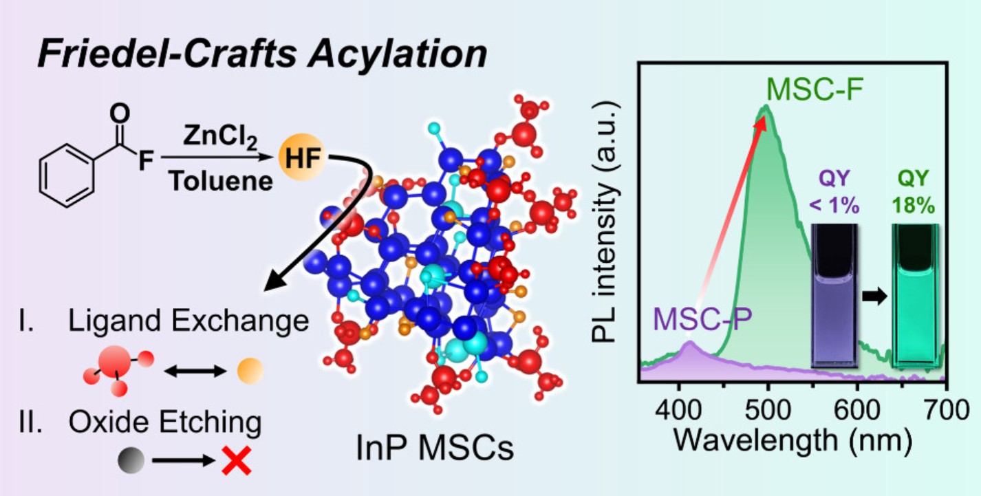
< Schematic illustration of overcoming emission efficiency limits via atomic-scale precision control >
As a result, the research team increased the luminescence efficiency of the semiconductor from below 1% to 18.1%. This represents the highest reported performance to date among indium phosphide–based ultrasmall nanosemiconductors, corresponding to an 18-fold increase in brightness.
This study is particularly significant in that it demonstrates, for the first time, that the surfaces of ultrasmall semiconductors—previously considered nearly impossible to control—can be precisely engineered at the atomic level. The technology is expected to find applications not only in next-generation displays, but also in advanced fields such as quantum communication and infrared sensing.

< Eco-friendly Ultra-compact Semiconductor Chemical Reaction (AI-generated image) >
Professor Himchan Cho explained, “This work is not simply about making brighter semiconductors, but about demonstrating how critical atomic-level surface control is for achieving desired performance.”
This research was carried out with Changhyun Joo, a doctoral student, and Seongbeom Yeon, a combined master’s-doctoral student in the Department of Materials Science and Engineering at KAIST, serving as co–first authors. Professor Himchan Cho and Professor Ivan Infante of the Basque Center for Materials, Applications, and Nanostructures (BCMaterials, Spain) participated as co-corresponding authors. The study was published online on December 16 in the Journal of the American Chemical Society (JACS), one of the most prestigious journals in chemistry.
※ Paper title: “Overcoming the Luminescence Efficiency Limitations of InP Magic-Sized Clusters,” DOI: 10.1021/jacs.5c13963
This research was supported by the National Research Foundation of Korea through the Nano Materials Technology Development Program, the Next-Generation Intelligent Semiconductor Technology Development Program, the Quantum Information Science Human Infrastructure Program, and by the Korea Basic Science Institute through its Infrastructure Support Program for Early-Career Researchers.
-
research KAIST Controls Where 2D Semiconductor Crystals Begin to Grow, Addressing a Key Challenge in Stacking AI Chips
Two-dimensional (2D) semiconductors, only a few atomic layers thick, are a promising material for making AI chips faster and more energy efficient by stacking additional semiconductor layers on top of existing computing circuits. However, when crystals form at multiple random locations during growth, it is difficult to produce high-quality semiconductors at the desired positions. A KAIST joint research team has developed a technology that sets in advance where a crystal begins to grow and allo
2026-10-13 -
research KAIST Develops AI Chip That Recognizes Changes in Motion over Time
For a wearable device to distinguish walking from a brief swing of the arm, it must recognize how a movement changes over time. Korean researchers have developed a technology that stacks semiconductor devices with different response speeds, allowing them to recognize both a change that has just occurred and the changes before it. The technology could be applied to small devices that are worn on or attached to the body to analyze movement and physiological signals. KAIST (President Choongsik B
2026-09-29 -
research KAIST Extends Lifespan of Graphite-Free Anode-Free Batteries That Could Make EV Batteries Smaller and Lighter
Korean researchers have developed a technology that could make electric-vehicle (EV) batteries smaller and lighter while helping EVs travel farther on a single charge. A KAIST research team has proposed a new solution to a persistent problem in anode-free batteries, which reduce weight and volume by eliminating anode materials such as graphite that normally store lithium during charging. In these batteries, lithium can grow into sharp, spike-like structures that shorten battery life. The key l
2026-09-22 -
research Single Material Enables Efficient Charge Injection into Two Types of Ultrathin Semiconductors, Paving the Way for Smaller, More Energy-Efficient AI Chips
A new approach could help make future AI chips smaller and more energy-efficient. A KAIST-led research team has used a single material to address one of the major obstacles facing atomically thin semiconductors, the difficulty of efficiently injecting charge. The technology could contribute to next-generation AI and low-power semiconductor devices in which multiple ultrathin layers are vertically integrated to increase device density and performance. KAIST (President Choongsik Bae) announced
2026-09-16 -
research KAIST Tames a Semiconductor Greenhouse Gas 6,000 Times More Potent Than CO₂ with the ‘Power of Disorder’
Among the gases used in semiconductor manufacturing, tetrafluoromethane (CF₄) is a greenhouse gas over 6,000 times more potent than carbon dioxide. A KAIST research team has developed a technology that removes this gas with high efficiency while extending the usable lifetime of the catalyst that helps break it down by harnessing the ‘power of disorder,’ in which mixing multiple metal atoms together actually stabilizes the catalyst’s structure. KAIST (President Choongsik Bae)
2026-09-03