research
- A KAIST research team led by Professor Keon Jae Lee demonstrates the transfer printing of a large number of micro-sized inorganic semiconductor chips via the selective modulation of micro-vacuum force.
MicroLEDs are a light source for next-generation displays that utilize inorganic LED chips with a size of less than 100 μm. MicroLEDs have attracted a great deal of attention due to their superior electrical/optical properties, reliability, and stability compared to conventional displays such as LCD, OLED, and QD. To commercialize microLEDs, transfer printing technology is essential for rearranging microLED dies from a growth substrate onto the final substrate with a desired layout and precise alignment. However, previous transfer methods still have many challenges such as the need for additional adhesives, misalignment, low transfer yield, and chip damage.
Professor Lee’s research team has developed a micro-vacuum assisted selective transfer printing (µVAST) technology to transfer a large number of microLED chips by adjusting the micro-vacuum suction force.
The key technology relies on a laser-induced etching (LIE) method for forming 20 μm-sized micro-hole arrays with a high aspect ratio on glass substrates at fabrication speed of up to 7,000 holes per second. The LIE-drilled glass is connected to the vacuum channels, controlling the micro-vacuum force at desired hole arrays to selectively pick up and release the microLEDs. The micro-vacuum assisted transfer printing accomplishes a higher adhesion switchability compared to previous transfer methods, enabling the assembly of micro-sized semiconductors with various heterogeneous materials, sizes, shapes, and thicknesses onto arbitrary substrates with high transfer yields.
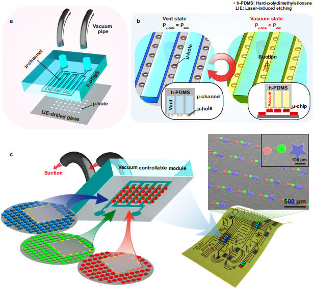
< Figure 01. Concept of micro-vacuum assisted selective transfer printing (μVAST). >
Professor Keon Jae Lee said, “The micro-vacuum assisted transfer provides an interesting tool for large-scale, selective integration of microscale high-performance inorganic semiconductors. Currently, we are investigating the transfer printing of commercial microLED chips with an ejector system for commercializing next-generation displays (Large screen TVs, flexible/stretchable devices) and wearable phototherapy patches.”
This result titled “Universal selective transfer printing via micro-vacuum force” was published in Nature Communications on November 26th, 2023. (DOI: 10.1038/S41467-023-43342-8)
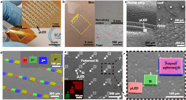
< Figure 02. Universal transfer printing of thin-film semiconductors via μVAST. >
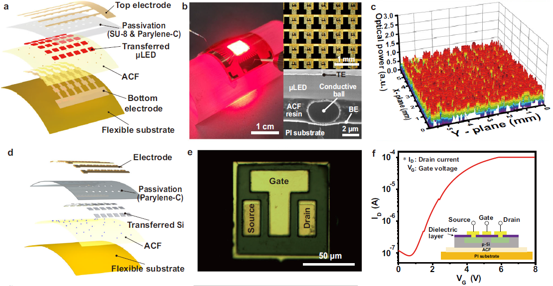
< Figure 03. Flexible devices fabricated by μVAST. >
Title: Entire process including LIE and µVAST
Vimeo link: https://vimeo.com/894430416?share=copy
-
research KAIST Develops Sodium Battery Capable of Rapid Charging in Just a Few Seconds
Sodium (Na), which is over 500 times more abundant than lithium (Li), has recently garnered significant attention for its potential in sodium-ion battery technologies. However, existing sodium-ion batteries face fundamental limitations, including lower power output, constrained storage properties, and longer charging times, necessitating the development of next-generation energy storage materials. On the 11th of April, KAIST (represented by President Kwang Hyung Lee) announced that a research t
2024-04-18 -
research KAIST introduces microbial food as a strategy food production of the future
The global food crisis is increasing due to rapid population growth and declining food productivity to climate change. Moreover, today's food production and supply system emit a huge amount of carbon dioxide, reaching 30% of the total amount emitted by humanity, aggravating climate change. Sustainable and nutritious microbial food is attracting attention as a key to overcoming this impasse. KAIST (President Kwang Hyung Lee) announced on April 12th that Research Professor Kyeong Rok Choi of th
2024-04-12 -
research KAIST researchers developed a novel ultra-low power memory for neuromorphic computing
A team of Korean researchers is making headlines by developing a new memory device that can be used to replace existing memory or used in implementing neuromorphic computing for next-generation artificial intelligence hardware for its low processing costs and its ultra-low power consumption. KAIST (President Kwang-Hyung Lee) announced on April 4th that Professor Shinhyun Choi's research team in the School of Electrical Engineering has developed a next-generation phase change memory* device fe
2024-04-04 -
research A KAIST-SNUH Team Devises a Way to Make Mathematical Predictions to find Metabolites Related to Somatic Mutations in Cancers
Cancer is characterized by abnormal metabolic processes different from those of normal cells. Therefore, cancer metabolism has been extensively studied to develop effective diagnosis and treatment strategies. Notable achievements of cancer metabolism studies include the discovery of oncometabolites* and the approval of anticancer drugs by the U.S. Food and Drug Administration (FDA) that target enzymes associated with oncometabolites. Approved anticancer drugs such as ‘Tibsovo (active ingre
2024-03-18 -
research KAIST Develops Healthcare Device Tracking Chronic Diabetic Wounds
A KAIST research team has developed an effective wireless system that monitors the wound healing process by tracking the spatiotemporal temperature changes and heat transfer characteristics of damaged areas such as diabetic wounds. On the 5th of March, KAIST (represented by President Kwang Hyung Lee) announced that the research team led by Professor Kyeongha Kwon from KAIST’s School of Electrical Engineering, in association with Chung-Ang University professor Hanjun Ryu, developed digit
2024-03-11