research
- Researchers calculate the quasi-Fermi levels in molecular junctions applying an initio approach. -
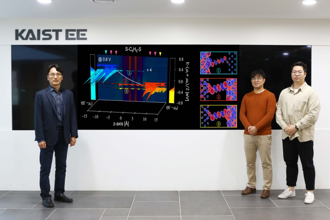
< Professor Yong-Hoon Kim (left), and PhD candidates Juho Lee (center) and Hyeonwoo Yeo (right) >
Semiconductor companies are struggling to develop devices that are mere nanometers in size, and much of the challenge lies in being able to more accurately describe the underlying physics at that nano-scale. But a new computational approach that has been in the works for a decade could break down these barriers.
Devices using semiconductors, from computers to solar cells, have enjoyed tremendous efficiency improvements in the last few decades. Famously, one of the co-founders of Intel, Gordon Moore, observed that the number of transistors in an integrated circuit doubles about every two years—and this ‘Moore’s law’ held true for some time.
In recent years, however, such gains have slowed as firms that attempt to engineer nano-scale transistors hit the limits of miniaturization at the atomic level.
Researchers with the School of Electrical Engineering at KAIST have developed a new approach to the underlying physics of semiconductors.
“With open quantum systems as the main research target of our lab, we were revisiting concepts that had been taken for granted and even appear in standard semiconductor physics textbooks such as the voltage drop in operating semiconductor devices,” said the lead researcher Professor Yong-Hoon Kim. “Questioning how all these concepts could be understood and possibly revised at the nano-scale, it was clear that there was something incomplete about our current understanding.”
“And as the semiconductor chips are being scaled down to the atomic level, coming up with a better theory to describe semiconductor devices has become an urgent task.”
The current understanding states that semiconductors are materials that act like half-way houses between conductors, like copper or steel, and insulators, like rubber or Styrofoam. They sometimes conduct electricity, but not always. This makes them a great material for intentionally controlling the flow of current, which in turn is useful for constructing the simple on/off switches—transistors—that are the foundation of memory and logic devices in computers.
In order to ‘switch on’ a semiconductor, a current or light source is applied, exciting an electron in an atom to jump from what is called a ‘valence band,’ which is filled with electrons, up to the ‘conduction band,’ which is originally unfilled or only partially filled with electrons. Electrons that have jumped up to the conduction band thanks to external stimuli and the remaining ‘holes’ are now able to move about and act as charge carriers to flow electric current.
The physical concept that describes the populations of the electrons in the conduction band and the holes in the valence band and the energy required to make this jump is formulated in terms of the so-called ‘Fermi level.’ For example, you need to know the Fermi levels of the electrons and holes in order to know what amount of energy you are going to get out of a solar cell, including losses.
But the Fermi level concept is only straightforwardly defined so long as a semiconductor device is at equilibrium—sitting on a shelf doing nothing—and the whole point of semiconductor devices is not to leave them on the shelf.
Some 70 years ago, William Shockley, the Nobel Prize-winning co-inventor of the transistor at the Bell Labs, came up with a bit of a theoretical fudge, the ‘quasi-Fermi level,’ or QFL, enabling rough prediction and measurement of the interaction between valence band holes and conduction band electrons, and this has worked pretty well until now.
“But when you are working at the scale of just a few nanometers, the methods to theoretically calculate or experimentally measure the splitting of QFLs were just not available,” said Professor Kim.
This means that at this scale, issues such as errors relating to voltage drop take on much greater significance.
Kim’s team worked for nearly ten years on developing a novel theoretical description of nano-scale quantum electron transport that can replace the standard method—and the software that allows them to put it to use. This involved the further development of a bit of math known as the Density Functional Theory that simplifies the equations describing the interactions of electrons, and which has been very useful in other fields such as high-throughput computational materials discovery.
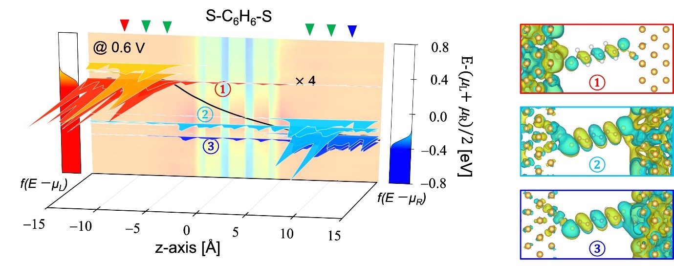
For the first time, they were able to calculate the QFL splitting, offering a new understanding of the relationship between voltage drop and quantum electron transport in atomic scale devices.
In addition to looking into various interesting non-equilibrium quantum phenomena with their novel methodology, the team is now further developing their software into a computer-aided design tool to be used by semiconductor companies for developing and fabricating advanced semiconductor devices.
The study, featured at the Proceedings of the National Academy of Sciences of the USA on May 12, was supported by the National Research Foundation and the Korea Institute of Science and Technology Information Supercomputing Center.
< Newly developed formalism and QFL splitting analysis. >
Image caption: The newly developed formalism and QFL splitting analysis led to new ways of characterizing extremely scaled-down semiconductor devices and the technology computer-aided design (TCAD) of next- generation nano-electronic/energy/bio devices.
Image credit: Yong-Hoon Kim, KAIST
Image usage restrictions: News organizations may use or redistribute this image, with proper attribution, as part of news coverage of this paper only.
Publication:
Juho Lee, Hyeonwoo Yeo, and Yong-Hoon Kim. (2020) ‘Quasi-Fermi level splitting in nanoscale junctions from ab initio.’ Proceedings of the National Academy of Sciences of the United States of America (PNAS), Volume 117, Issue 19, pp.10142-101488. Available online at https://doi.org/10.1073/pnas.1921273117
Profile:
Yong-Hoon Kim
Professor
y.h.kim@kaist.ac.kr
http://nanocore.kaist.ac.kr/
1st-Principles Nano-Device Computing Lab
School of Electrical Engineering
KAIST
(END)
-
research KAIST Researchers Suggest an Extraordinary Alternative to Petroleum-based PET - Bacteria!
< (From left) Dr. Cindy Pricilia, Ph.D. Candidate Cheon Woo Moon, Distinguished Professor Sang Yup Lee > Currently, the world is suffering from environmental problems caused by plastic waste. The KAIST research team has succeeded in producing a microbial-based plastic that is biodegradable and can replace existing PET bottles, making it a hot topic. Our university announced on the 7th of November that the research team of Distinguished Professor Sang Yup Lee of the Department of Ch
2024-11-08 -
research Mystery Solved with Math: Cytoplasmic Traffic Jam Disrupts Sleep-Wake Cycles
KAIST mathematicians and their collaborators at Florida State University have identified the principle of how aging and diseases like dementia and obesity cause sleep disorders. A combination of mathematical modelling and experiments demonstrated that the cytoplasmic congestion caused by aging, dementia, and/or obesity disrupts the circadian rhythms in the human body and leads to irregular sleep-wake cycles. This finding suggests new treatment strategies for addressing unstable sleep-wake cycles
2020-12-11 -
research Drawing the Line to Answer Art’s Big Questions
- KAIST scientists show how statistical physics can reveal art trends across time and culture. - Algorithms have shown that the compositional structure of Western landscape paintings changed “suspiciously” smoothly between 1500 and 2000 AD, potentially indicating a selection bias by art curators or in art historical literature, physicists from the Korea Advanced Institute of Science and Technology (KAIST) and colleagues report in the Proceedings of the National Academy of Sciences
2020-11-13 -
research To Talk or Not to Talk: Smart Speaker Determines Optimal Timing to Talk
A KAIST research team has developed a new context-awareness technology that enables AI assistants to determine when to talk to their users based on user circumstances. This technology can contribute to developing advanced AI assistants that can offer pre-emptive services such as reminding users to take medication on time or modifying schedules based on the actual progress of planned tasks. Unlike conventional AI assistants that used to act passively upon users’ commands, today’s A
2020-11-05 -
research X-ray Scattering Shines Light on Protein Folding
- Multiple forms of a non-functional, unfolded protein follow different pathways and timelines to reach its folded, functional state, a study reveals. - KAIST researchers have used an X-ray method to track how proteins fold, which could improve computer simulations of this process, with implications for understanding diseases and improving drug discovery. Their findings were reported in the Proceedings of the National Academy of Sciences of the United States of America (PNAS) on June 30. Whe
2020-07-09