research

< 20190221165451_14865_542598267.jpg >
(from left: Juho Lee, Dr. Muhammad Ejaz Khan and Professor Yong-Hoon Kim)
A KAIST research team reported a novel non-linear device with the founding property coming from perovskite nanowires. They showed that hybrid perovskite-derived, inorganic-framework nanowires can acquire semi-metallicity, and proposed negative differential resistance (NDR) devices with excellent NDR characteristics that resulted from a novel quantum-hybridization NDR mechanism, implying the potential of perovskite nanowires to be realized in next-generation electronic devices.
Organic-inorganic hybrid halide perovskites have recently emerged as prominent candidates for photonic applications due to their excellent optoelectronic properties as well as their low cost and facile synthesis processes. Prominent progresses have been already made for devices including solar cells, light-emitting diodes, lasers and photodetectors.
However, research on electronic devices based on hybrid halide perovskites has not been actively pursued compared with their photonic device counterparts.
Professor Yong-Hoon Kim from the School of Electrical Engineering and his team took a closer look at low-dimensional organic-inorganic halide perovskite materials, which have enhanced quantum confinement effects, and particularly focused on the recently synthesized trimethylsulfonium (TMS) lead triiodide (CH3)3SPbI3.
Using supercomputer simulations, the team first showed that stripping the (CH3)3S or TMS organic ligands from the TMS PbI3 perovskite nanowires results in semi-metallic PbI3 columns, which contradicts the conventional assumption of the semiconducting or insulating characteristics of the inorganic perovskite framework.
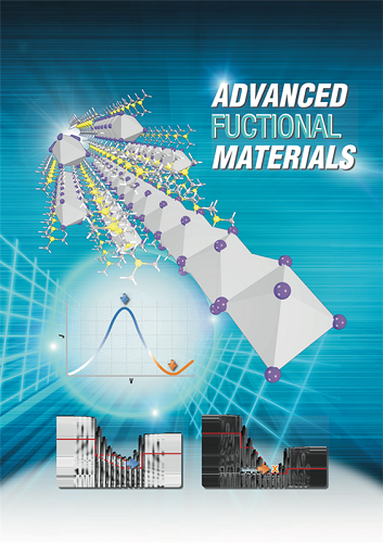
Utilizing the semi-metallic PbI3 inorganic framework as the electrode, the team designed a tunneling junction device from perovskite nanowires and found that they exhibit excellent nonlinear negative differential resistance (NDR) behavior. The NDR property is a key to realizing next-generation, ultra-low-power, and multivalued non-linear devices. Furthermore, the team found that this NDR originates from a novel mechanism that involves the quantum-mechanical hybridization between channel and electrode states.
Professor Kim said, “This research demonstrates the potential of quantum mechanics-based computer simulations to lead developments in advanced nanomaterials and nanodevices. In particular, this research proposes a new direction in the development of a quantum mechanical tunneling device, which was the topic for which the Nobel Laureate in Physics in 1973 was awarded to Dr. Leo Esaki.
This research, led by Dr. Muhammad Ejaz Khan and PhD candidate Juho Lee, was published online in Advanced Functional Materials (10.1002/adfm.201807620) on January 7, 2019.
Figure. The draft version of the cover page of 'Advanced Functional Materials'

-
research A Theoretical Boost to Nano-Scale Devices
- Researchers calculate the quasi-Fermi levels in molecular junctions applying an initio approach. - Semiconductor companies are struggling to develop devices that are mere nanometers in size, and much of the challenge lies in being able to more accurately describe the underlying physics at that nano-scale. But a new computational approach that has been in the works for a decade could break down these barriers. Devices using semiconductors, from computers to solar cells, have enjoyed tremend
2020-05-15 -
research Hierarchical Porous Titanium Nitride Synthesized by Multiscale Phase Separation for LSBs
(from left: Professor Jinwoo Lee and PhD candidate Won-Gwang Lim) A KAIST research team developed ultra-stable, high-rate lithium-sulfur batteries (LSBs) by using hierarchical porous titanium nitride as a sulfur host, and achieved superior cycle stability and high rate performance for LSBs. The control of large amounts of energy is required for use in an electric vehicle or smart grid system. In this sense, the development of next-generation secondary batteries is in high
2019-01-28 -
research Highly Scalable Process to Obtain Stable 2D Nanosheet Dispersion
(Professor Do Hyun Kim and his team) A KAIST team developed technology that allows the mass production of two-dimensional (2D) nanomaterial dispersion by utilizing the characteristic shearing force of hydraulic power. The 2D nanosheet dispersion can be directly applied to solution-based processes to manufacture devices for electronics as well as energy storage and conversion. It is expected to be used in these devices with improved performance. There have been numero
2018-12-19 -
research Characteristics of Submesoscale Geophysical Turbulence Reported
A KAIST research team has reported some of unique characteristics and driving forces behind submesoscale geophysical turbulence. Using big data analysis on ocean surface currents and chlorophyll concentrations observed using coastal radars and satellites has brought better understanding of oceanic processes in space and time scales of O(1) kilometer and O(1) hour. The outcomes of this work will lead to improved tracking of water-borne materials and performance in global and regional climate
2018-12-13 -
research Silk Adhesive Paves the Way for Epidermal Electronics
(from left: Dr. Ji-Won Seo, Professor Hyunjoo Jenny Lee and PhD candidate, Hyojung Kim) Producing effective epidermal electronics requires a strong, biocompatible interface between a biological surface and a sensor. Here, a KAIST team employed a calcium-modified silk fibroin as a biocompatible and strong adhesive. This technology led to the development of epidermal electronics with strong adhesion for patients who need drug injections and physiological monitoring over a long
2018-11-21