research
IBS & KAIST researchers clarify how laser annealing technology can lead to the production of ultrathin nanomaterials
All our smart phones have shiny flat AMOLED (active-matrix organic light-emitting diode) displays. Behind each single pixel of these displays hides at least two silicon transistors which are mass-manufactured using laser annealing technology. While the traditional methods to make the transistors use temperature above 1,000°C, the laser technique reaches the same results at low temperatures even on plastic substrates (melting temperature below 300°C). Interestingly, a similar procedure can be used to generate crystals of graphene. Graphene is a strong and thin nano-material made of carbon, its electric and heat-conductive properties have attracted the attention of scientists worldwide.
Professor Keon Jae Lee of the Materials Science and Engineering Department at KAIST and his research group at the Center for Multidimensional Carbon Materials within the Institute for Basic Science (IBS), as well as Professor Sung-Yool Choi of the Electrical Engineering School at KAIST and his research team discovered graphene synthesis mechanism using laser-induced solid-state phase separation of single-crystal silicon carbide (SiC). This study, available in Nature Communications, clarifies how this laser technology can separate a complex compound (SiC) into its ultrathin elements of carbon and silicon.
Although several fundamental studies presented the effect of excimer lasers in transforming elemental materials like silicon, the laser interaction with more complex compounds like SiC has rarely been studied due to the complexity of compound phase transition and ultra-short processing time.
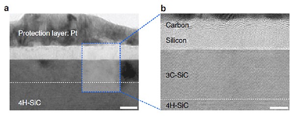
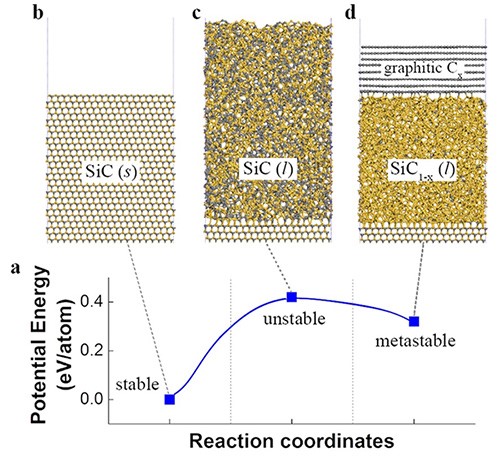
With high resolution microscope images and molecular dynamic simulations, scientists found that a single-pulse irradiation of xenon chloride excimer laser of 30 nanoseconds melts SiC, leading to the separation of a liquid SiC layer, a disordered carbon layer with graphitic domains (about 2.5 nm thick) on top surface and a polycrystalline silicon layer (about 5 nm) below carbon layer. Giving additional pulses causes the sublimation of the separated silicon, while the disordered carbon layer is transformed into a multilayer graphene.
"This research shows that the laser material interaction technology can be a powerful tool for the next generation of two dimensional nanomaterials," said Professor Lee.
Professor Choi added: "Using laser-induced phase separation of complex compounds, new types of two dimensional materials can be synthesized in the future."

High-resolution transmission electron microscopy shows that after just one laser pulse of 30 nanoseconds, the silicon carbide (SiC) substrate is melted and separates into a carbon and a silicon layer. More pulses cause the carbon layer to organize into graphene and the silicon to leave as gas.

Molecular dynamics simulates the graphene formation mechanism. The carbon layer on the top forms because the laser-induced liquid SiC (SiC (l)) is unstable.
(Press Release by Courtesy of the Institute for Basic Science (IBS))
-
research KAIST developed a plastic film board less sensitive to heat.
The research result was made the cover of magazine, Advanced Materials and is accredited to paving the way to commercialize flexible display screens and solar power cells. Transparent plastic and glass cloths, which have a limited thermal expansion needed for the production of flexible display screens and solar power cells, were developed by Korean researchers. The research, led by KAIST’s Professor Byoung-Soo Bae, was funded by the Engineering Research Center under the initiativ
2011-01-05 -
people Youngseok Son and Yongjoon Chun won a prize of Commerce, Industry and Energy Minister
Youngseok Son and Yongjoon Chun won a prize of Commerce, Industry and Energy Minister Youngseok Son and Yongjoon Chun, doctorate students at circuit design and system application lab of Electrical Engineering Division, won a prize of Commerce, Industry and Energy Minister (Silver prize) at the 7th Semiconductor Design Contest hosted by the Korean Intellectual Property Office. Their work exhibited at the contest is ‘a driving circuit for the improvement of image quality of AMOLED disp
2006-11-27